Overview and production process characteristICs of carbon film PCB
PCB manufacturing, PCB design and PCBA processing manufacturers will explain the overview and production process characteristics of carbon film PCB
There are two common methods of making circuit in printed circuit board: subtraction method and addition method. The addition method uses electrolytic free or electroplated copper to generate circuits. The method of using conductive ink is one of the addition methods. The conductive ink is used to make wires and printed on insulators to generate circuits. This method is relatively easy and effective to produce printed circuits of various shapes.
The production process of carbon film PCB is a PCB manufacturing method that combines the subtractive method and the additive method.

At present, carbon film printed boards have made breakthrough progress in the field of application, especially in electronic products with low electrical power. As a permanent conductive coating on printed boards, carbon film printed boards have been adopted and promoted by many electronIC designers.
With the rapid development of the electronic industry, carbon film PCB is gradually adopted in the daily electrical appliances and instruments towards multi-function and miniaturization. Such as: TV, telephone, electronic organ, game machine, video recorder, etc. Its new technologies and functions have been continuously developed and utilized. The electronic fields of computer keyboards, card type computing machines, micro radio recorders, electronic measuring devices and SMT have also started to select carbon film printed boards, thus improving its reputation and expanding its demand.
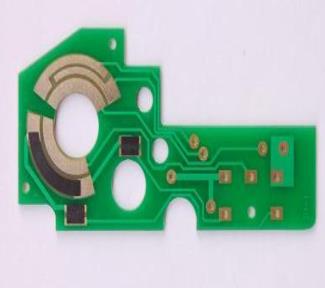
The carbon film PCB uses a SIMple screen printing process to add one or two layers of conductive graphics on a single side printed board to achieve high-density wiring. The printed conductive graphics are not only used as interconnection wires, but also used as resistors, key switch contacts, electromagnetic shielding layers, etc.
This process has the advantages of both empty metallized PCB and single-sided PCB, forming a single-sided double-layer PCB without interconnection holes; Simplify the production process of porous metallized printed boards, which can be directly printed through screen printing and can be easily mastered; Light weight, thinness can be realized, even phenolic paperboard can be used; Parts installation holes can also be blanking processed; Adapt to mass production, shorten the production cycle, production costs, no three waste pollution.
Carbon film PCB can shorten the production cycle of double-sided boards by two-thirds; The volume of the whole machine is reduced by one quarter to one third; The assembly efficiency of the whole machine is increased by 30%; The production cost is reduced by one third, and more double-sided porous boards or simple multilayer boards are converted to the carbon film PCB production mode.
As far as the technical specifications of carbon film printed boards are concerned, some technical descriptions of conductive coatings in IEC1249-5-4; Famous companies have also developed some technical specifications for carbon film PCB; Some ink manufacturers. There are also technical conditions for conductive ink; But these are only some simple descriptions and introductions; In 1998, SJ/T11171-98 Specification for Non metallized Single and Double Sided Carbon Film Printed Boards issued by China's electronic industry comprehensively discussed the technical conditions and test methods of carbon film boards. PCB manufacturers, PCB designers and PCBA manufacturers will explain the overview and production process characteristics of carbon film PCB.


