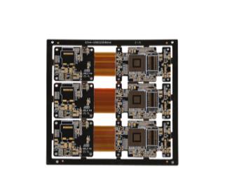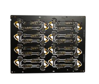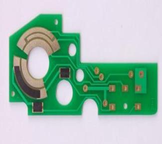
Advantages and Problems of Embedded Passive Component Circuit Boards
PCB manufacturers, PCB designers and PCBA manufacturers explain the advantages and problems of embedded passive component PCB
Due to the rapid development of electronIC products towards miniaturization and multi-function, it is required to reduce the number of discrete passive components assembLED and the size of PCB as much as possible, while increasing the functionality of PCB, better reliability and lower product cost. Therefore, a large number of embeddable passive components are embedded in the circuit board (HDI/BUM), so that the components after PCB assembly have the following advantages:
1: Improve PCB high-density
Because discrete (non embedded) passive components not only have a large number of assemblies, but also occupy a large amount of space on the PCB board. For example, if the GSM phone (or HDI/BUM) is calculated internally, the size of the PCB board can be reduced by about 25%. Thus, the number of through holes is greatly reduced, and the connecting lines are reduced and shortened. It can not only increase the flexibility and freedom of PCB design wiring, but also reduce the wiring and shorten the length of wiring, thus greatly improving the high-density degree of PCB (or HDI/BUM).

2: Improve the high reliability of PCB assembly
The reliability of PCB (or HDI/BUM) assembly can be significantly improved by embedding the required passive components into the PCB. Based on two aspects: First, through this process method, the solder joints on the PCB surface are significantly reduced, thereby improving the reliability of the assembly board and greatly reducing the probability of failure caused by solder joints.
Second, the embedded passive components can receive effective "protection" and improve the reliability. Because these embedded passive components are embedded in the PCB as a whole, unlike discrete (or dispersed) passive components, which are welded (or bonded) to the connecting pad on the PCB board with a leg, they will not be eroded by moisture and harmful gases in the atmOSPhere, reducing or damaging the passive components. Therefore, the way of embedding passive components is to significantly improve the reliability of PCB assembly, which is a very effective process method.
3: Improve the electrical performance of PCB assemblies
By embedding passive components in high-density PCB, the electrical performance of electronic interconnects has been significantly improved. This is because it eliminates the circuit formed by welding the connecting pads, wires and their own leads required by discrete passive components. Any such circuit will inevitably produce parasitic effects, namely stray capacitance and parasitic inductance. And this parasitic effect will become more serious with the increase of frequency or pulse front time. Eliminating this type of fault will undoubtedly improve the electrical performance of PCB assemblies. At the same time, it also improves the stability of passive component functions and reduces the failure of passive component functions. Because the passive components are embedded in the PCB, and the surrounding areas are tightly protected, their function values will not be changed due to dynamic changes in the working environment, making them in a very stable state.
4: Saving product manufacturing cost
By adopting this process method, the cost of products or PCB assemblies can be significantly saved. For example, in the model study of EP-RF, the PCB substrate equivalent to LTCC can save 10% of the component cost, 30% of the substrate cost, and 40% of the assembly cost. At the same time, because the assembly process and sintering process of ceramic substrate are difficult to control, and the embedded passive components of PCB substrate can be completed using traditional PCB manufacturing process, thus greatly improving the production efficiency.
Of course, any public welfare method has certain limitations. First, it needs to develop embedded passive component materials with large functional values for the resistance, capacitance and inductance values of passive components with large functional values; The second is that it is difficult to control the functional error of the embedded passive components, especially the functional error control of the planar embedded passive component materials with screen leakage. At present, although laser technology is used to trim and control the functional error of embedded passive components, not all embedded passive components can be trimmed by this method to meet the design technical requirements. PCB manufacturers, PCB designers and PCBA manufacturers will explain the advantages and problems of embedded passive component PCB.


