PCB high-frequency board resistance welding process often encounters problems
PCB manufacturers, PCB designers and PCBA manufacturers explain some problems often encountered in the solder resistance process of PCB high-frequency boards
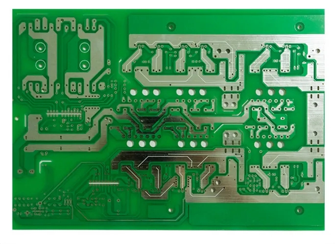
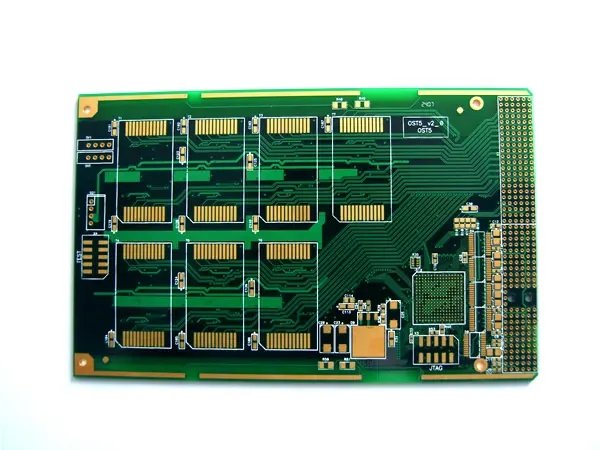
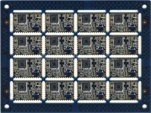
Everyone in the PCB high-frequency board design industry knows that solder mask is a layer of ink printed on the surface of the PCB high-frequency board. It not only plays the role of insulation, but also plays the role of protecting the copper surface, and also plays a beautiful role. It is like a piece of clothing worn outside the PCB high-frequency board. Therefore, any flaw in it is very easy to be found, so solder mask is also the process most likely to cause customer complaints in all processes. In the resistance welding process of PCB high-frequency boards, you may also encounter a variety of quality problems. The following sections summarize the countermeasures for some common problems, hoping to give you inSPIration and help. Common:

Problem: PCB high-frequency board penetration and blurring
Cause 1: Ink viscosity is too low.
Improvement measures: increase the concentration without adding thinner.
Cause 2: High frequency PCB screen pressure is too high.
Improvement measures: reduce the pressure.
Cause 3: The rubber scraper is poor.
Improvement measures: replace or change the angle of the squeegee screen.
Cause 4: The distance between the high-frequency PCB screen and the printed surface is too large or too SMAll.
Improvement measures: adjust the spacing.
Cause 5: The tension of the screen on the high-frequency PCB board decreases
Improvement measures: Make new screen version.
Problem: Viscous film
Cause 1: PCB high-frequency board ink is not baked dry
Improvement measures: check the ink dryness
Cause 2: Too strong vacuum pumping
Improvement measures: check the vacuum pumping system (air guide strip may not be added)
Problem: Poor exposure
Cause 1: Poor vacuum pumping
Improvement measures: check the vacuum pumping system
Cause 2: Improper exposure energy
Improvement measures: adjust appropriate exposure energy
Cause 3: The temperature of the exposure machine is too high
Improvement measures: check the temperature of the exposure machine (lower than 26 ℃)
Problem: The ink won't dry
Cause 1: Poor ventilation of the oven
Improvement measures: check the air exhaust condition of the oven
Cause 2: InsuffICient oven temperature
Improvement measures: determine whether the actual temperature of the oven reaches the required temperature of the product
Cause 3: Thinner is not enough
Improvement measures: add thinner and fully dilute
Cause 4: Thinner dries too slowly
Improvement measures: use the matching thinner [please use the company's matching thinner]
Cause 5: The ink is too thick
Improvement measures: appropriately adjust the ink thickness
Problem: There are white dots in the printing
Cause 1: There are white dots in the printing
Improvement measures: The thinner does not match. Use the matching thinner [please use the company's matching thinner]
Cause 2: The sealing tape is dissolved
Improvement measures: use white paper to seal the net
Problem: Excessive development (corrosion measurement)
Cause 1: Too high concentration and temperature of liquid medicine
Improvement measures: reduce the concentration and temperature of liquid medicine
Cause 2: Development time is too long
Improvement measures: shorten the development time
Cause 3: Insufficient exposure energy
Improvement measures: increase exposure energy
Cause 4: Excessive developing water pressure
Improvement measures: reduce the pressure of developing water
Cause 5: uneven mixing of ink
Improvement measures: Stir the ink evenly before printing
Cause 6: PCB high-frequency board ink is not dried
Improvement measures: adjust the baking parameters, see the problem [Ink does not dry]
Problem: Green Oil Bridge is broken
Cause 1: Insufficient exposure energy
Improvement measures: increase exposure energy
Cause 2: PCB high-frequency boards were not handLED properly
Improvement measures: check the processing procedure
Cause 3: Too much developing and washing pressure
Improvement measures: check the developing and washing pressure
Problem: Unclean development
Cause 1: PCB high-frequency board is placed for too long after printing
Improvement measures: control the storage time within 24 hours
Cause 2: Ink runs out before development
Improvement measures: work in the darkroom before development (fluorescent lamps are wrapped in yellow paper)
Cause 3: Insufficient developer solution
Improvement measures: if the temperature is not enough, check the concentration and temperature of liquid medicine
Cause 4: Development time is too short
Improvement measures: extend the development time
Cause 5: High exposure energy
Improvement measures: adjust exposure energy
Cause 6: Excessive baking of ink
Improvement measures: adjust baking parameters to prevent baking
Cause 7: uneven mixing of ink
Improvement measures: Stir the ink evenly before printing
Cause 8: Diluent mismatch
Improvement measures: use the matching thinner [please use the company's matching thinner]
Problem: Poor tin coating
Cause 1: Unclean development
Improvement measures: several factors to improve the development uncleanness
Cause 2: Post baking solvent pollution
Improvement measures: increase oven exhaust or machine cleaning before tin spraying
Problem: post drying and exploding oil
Cause 1: No segmental baking
Improvement measures: baking in sections
Cause 2: The viscosity of the plug hole ink is not enough
Improvement measures: adjust the ink viscosity of the plug hole
Problem: blistering on tin
Cause 1: Overdevelopment
Improvement measures: improve the development parameters, see the problem [Excessive development]
Cause 2: The pretreatment of the plate is not good, and the surface is greasy. Dust
Improvement measures: do a good job in the pretreatment of plates and keep the surface clean
Cause 3: Insufficient exposure energy
Improvement measures: check the exposure energy to ensure it meets the requirements for ink use
Cause 4: Abnormal flux
Improvement measures: adjust the flux
Cause 5: Insufficient post baking
Improvement measures: post inspection baking process
Problem: Ink discoloration
Cause 1: Insufficient ink thickness
Improvement measures: increase the ink thickness
Cause 2: substrate oxidation
Improvement measures: pre inspection processing procedure
Cause 3: The post baking temperature is too high
Improvement measures: too long to check the baking parameters
Problem: Matte ink
Cause 1: Diluent mismatch
Improvement measures: use the matching thinner [please use the company's matching thinner]
Cause 2: Low exposure energy
Improvement measures: increase exposure energy
Cause 3: Excessive development of PCB high-frequency board
Improvement measures: improve the development parameters, see the problem [Excessive development]
Problem: blocking
Cause 1: Too fast drying.
Improvement measures: add slow drying agent.
Reason 2: The printing speed is too slow.
Improvement measures: increase the speed and slow the drying agent.
Cause 3: The ink viscosity is too high.
Improvement measures: add ink lubricant or extra slow drying agent.
Cause 4: Diluent is not suitable.
Improvement measures: use the specified thinner.
Problem: The ink adhesion is not strong
Cause 1: The model of PCB high-frequency board ink is not suitable.
Improvement measures: change to appropriate ink.
Cause 2: The model of PCB high-frequency board ink is not suitable.
Improvement measures: change to appropriate ink.
Cause 3: The drying time and temperature are incorrect and the exhaust air volume during drying is too small.
Improvement measures: use correct temperature and time, and increase exhaust air volume.
Cause 4: The dosage of additives is inappropriate or incorrect.
Improvement measures: adjust the dosage or use other additives.
Cause 5: Excessive humidity.
Improvement measures: improve the air dryness.
PCB manufacturers, PCB designers and PCBA manufacturers explain some problems often encountered in the resistance welding process of PCB high-frequency boards.


