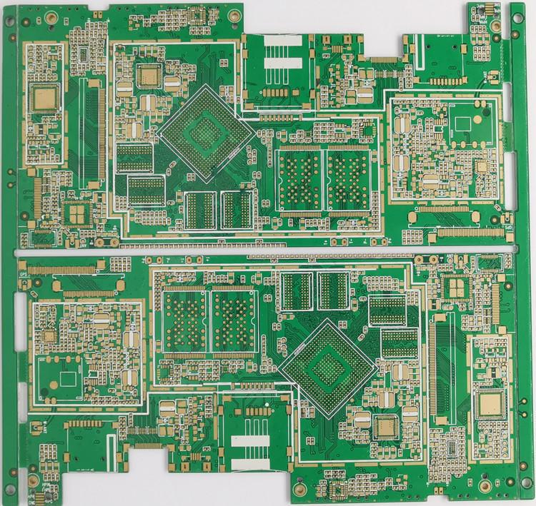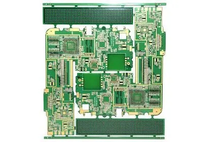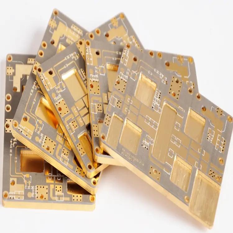
The Harm and Cause Analysis of PCB High Frequency Circuit Board Deformation
PCB manufacturers, PCB designers and PCBA manufacturers explain the hazards and causes of PCB high-frequency circuit board deformation
In the automatIC surface mounting line, if the circuit board is not flat, it will cause inaccurate positioning, and components cannot be inserted or mounted on the holes and surface mounting pads of the high-frequency circuit board, or even damage the automatic insertion machine. The circuit board with components is bent after welding, and it is difficult to cut the component legs neatly. High Frequency Circuit Board can not be instalLED on the chassis or the socket inside the machine, so it is also very troublesome for the assembly plant to encounter the board warping.
At present, Surface Mount Technology is developing towards high precision, high speed and intelligence, which puts forward higher flatness requirements for PCB high-frequency circuit boards as the home of various components.
In the IPC standard, it is specially pointed out that the allowable deformation of PCB high-frequency circuit board with surface mount devices is 0.75%, and the allowable deformation of PCB high-frequency circuit board without surface mount devices is 1.5%.
In fact, in order to meet the requirements of high-precision and high-speed mounting, some electronic assembly manufacturers have more stringent requirements on deformation. If required, the allowable deformation is 0.5%, or even 0.3% in some cases.

PCB high-frequency circuit board is composed of copper foil, resin, glass cloth and other materials. The physical and chEMIcal properties of each material are different. After pressing together, thermal stress residues will inevitably occur, leading to deformation.
At the same time, in the process of PCB processing, various processes such as high temperature, mechanical cutting, and wet treatment will also have an important impact on the deformation of the board. In short, the causes of PCB high-frequency circuit board deformation are complex and diverse. How to reduce or eliminate the deformation caused by different material properties or processing has become one of the complex problems faced by PCB manufacturers.
Cause Analysis of PCB High Frequency Circuit Board Deformation
The deformation of PCB high-frequency circuit board needs to be studied from several aspects such as material, structure, graphic distribution, processing process, etc. This paper will analyze and elaborate various causes of possible deformation and improvement methods.
The uneven copper surface area on the circuit board will worsen the bending and warping of the board.
Generally, a large area of copper foil is designed on the circuit board for grounding. Sometimes, a large area of copper foil is designed on the Vcc layer. When these large areas of copper foil cannot be evenly distributed on the same circuit board, the problem of uneven heat absorption and heat dissipation will occur.
Of course, the circuit board will also expand with heat and contract with cold. If the expansion and contraction can not SIMultaneously cause deformation due to different stresses, at this time, if the temperature of the high-frequency circuit board has reached the upper limit of Tg value, the high-frequency circuit board will begin to soften, causing deformation.
The connection points (vias) on each layer of the circuit board will limit the expansion and contraction of the high-frequency circuit board.
Nowadays, most circuit boards are multilayer boards, and there will be rivet like connection points (vias) between layers. The connection points are divided into through holes, blind holes and buried holes. Where there are connection points, the effect of expansion and contraction of high-frequency circuit boards will be limited, and the bending and warping of boards will be indirectly caused.
Reasons for PCB high-frequency circuit board deformation:
(1) The weight of the circuit board itself will cause the high-frequency circuit board to be concave and deformed
Generally, a chain is used in the reflow furnace to drive the circuit board to move forward in the reflow furnace, that is, both sides of the high-frequency circuit board are used as fulcrums to support the whole high-frequency circuit board.
If there are overweight parts on the high-frequency circuit board, or the size of the high-frequency circuit board is too large, it will show a depression in the middle due to its own weight, causing bending.
(2) The depth of V-Cut and the connecting bar will affect the deformation of the panel
Basically, V-Cut is the culprit of destroying the substructure of high-frequency circuit board. Because V-Cut cuts grooves on the original large sheet, the V-Cut area is prone to deformation.
Influence of pressing material, structure and figure on deformation of plate:
High frequency PCB circuit board is formed by pressing core board, semi solidified sheet and outer copper foil. The core board and copper foil are subject to thermal deformation during pressing, and the deformation amount depends on the thermal expansion coefficient (CTE) of the two materials.
The coefficient of thermal expansion (CTE) of copper foil is about 17X10-6; While the CTE of common FR-4 substrate in Z-direction at Tg point is (50~70) X10-6; Above TG point is (250~350) X10-6. Due to the existence of glass cloth, CTE in X direction is generally similar to copper foil. PCB manufacturers, PCB designers and PCBA manufacturers will explain the hazards and causes of PCB high-frequency PCB deformation.


