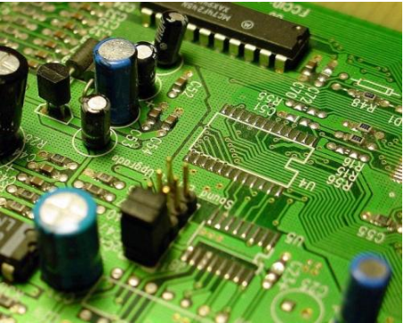
PCB proofing production PCB equipment judges the quality of PCB from PCB color. Buyers always have doubts about the color of PCB, and do not know what color PCB is of high quality. Today we will explain how the color of PCB affects its performance.
PCB proofing
First, as a printed circuit board, the pcb proofing PCB mainly provides the interconnection between electronIC components. Color is not directly related to performance, and different pigments will not affect electrICal properties. The performance of PCB is determined by the materials used (high Q value), wiring design and several layers of boards. However, in the process of PCB washing, black is the most likely to cause color difference. If there is a slight deviation between the raw materials used in the PCB factory and the manufacturing process, the color difference will cause an increase in the defective rate of PCB. This directly leads to increased production costs.

In fact, the raw materials of pcb proofing PCB are ubiquitous in our daily life, that is, glass fiber and resin. Glass fiber and resin are combined and hardened to become a kind of heat insulation, insulating, and not easy to bend plate, which is PCB substrate. Of course, the PCB substrate made of glass fiber and resin alone cannot transmit signals. Therefore, the manufacturer will cover the surface of the PCB substrate with a layer of copper, so the PCB substrate can also be calLED a copper clad substrate.
Because the circuit routing of pcb proofing black PCB is difficult to identify, it will increase the difficulty of maintenance and debugging in the R&D and after-sales stages. Generally, black PCB will not be used easily without the brand of skilled RD (R&D) personnel and powerful maintenance team. It can be said that the use of black PCB is a sign that a brand has confidence in RD design and post maintenance teams. From the side, it is also a reflection of the manufacturers' confidence in their own strength.
PCB
Based on the above reasons, all major manufacturers will carefully consider when selecting PCB design for their products. As a result, most of the products with large MARKet shipments in that year used red PCB, green PCB or blue PCB versions, and only the high-end or top flagship products could see black PCB, so customers should not think that black PCB is better than green PCB.
Prevent reflow problem in PCB production
The PCB is prone to bending and warping when passing through the reflow furnace. How to prevent the PCB from bending and warping when passing through the reflow furnace? Here's a detailed explanation for every 100 million PCBs:
1. Effect of temperature reduction on PCB stress
Since "temperature" is the main source of PCB stress, as long as the temperature of the reflow furnace is reduced or the heating and cooling speed of PCB production in the reflow furnace is slowed down, the occurrence of plate bending and warping can be greatly reduced. However, there may be other side effects, such as short circuit.
2. PCB adopts high Tg plate
Tg is the glass transition temperature, that is, the temperature at which the material changes from glass state to rubber state. The lower the Tg value of the material, the faster the circuit board begins to soften after entering the reflow furnace, and the longer the time to become soft rubber state will be, of course, the more serious the deformation of the circuit board will be. The use of boards with higher Tg can increase their ability to withstand stress and deformation, but the cost of PCB production is relatively high compared with that of materials to the ground.
3. Increase the thickness of PCB
In order to make many electronic products lighter and thinner, the thickness of the circuit board has remained 1.0mm, 0.8mm, or even 0.6mm. It is really difficult to keep the circuit board from deforming when it passes through the reflow furnace. It is recommended that if there is no requirement for thinness, the circuit board should be 1.6mm thick, which can greatly reduce the risk of bending and deformation.
PCB
4. Reduce the size of circuit boards and the number of boards
Since most of the reflow furnaces use chains to drive the circuit board forward, the circuit board with larger PCB design size will sag and deform in the reflow furnace due to its own weight, so try to put the long side of the circuit board on the chain of the reflow furnace as the board edge, which can reduce the sag and deformation caused by the weight of the circuit board itself. This is also the reason to reduce the number of panels, that is, when the furnace is said, The narrow edge shall be perpendicular to the furnace passing direction as far as possible to achieve the lowest concave deformation.
5. Use the furnace tray fixture
If the above methods are difficult to achieve, the last thing is to use the furnace tray to reduce the deformation. The reason why the furnace tray can reduce the bending warpage is that whether it is thermal expansion or cold contraction, it is hoped that the tray can fix the circuit board until the temperature of the circuit board is lower than the Tg value and it starts to harden again, and then it can maintain the round size.
If the single-layer tray cannot reduce the deformation of the circuit board, you must add another layer of cover to clamp the circuit board with two layers of trays, which can greatly reduce the deformation of the circuit board through the reflow furnace. However, this tray is very expensive, and it needs to be manually placed and recycled.
6. Replace V-Cut with Router
Since V-Cut will damage the structural strength of the panels between circuit boards, it is better not to use V-Cut to divide boards or reduce the depth of V-Cut. Professional PCB manufacturers and PCB design and solution service providers focus on the development of PCB industry and are trustworthy.


