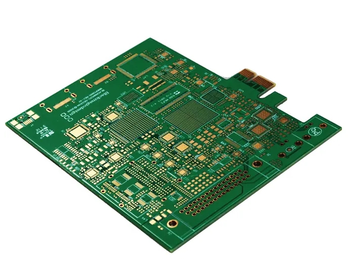
What problems will occur in PCB punching and the causes of blistering on the board surface
Punching is an important process in PCB proofing. What problems will occur in PCB punching? Now please follow the PCB engineer to understand.
1、 Rough section
1. Cause:
(1) The blanking clearance of concave and convex dies is too large; The cutting edge of the female die is seriously worn.
(2) The blanking force of the punch is insuffICient and unstable.
(3) The blanking performance of sheet metal is poor.
2. Solution:
(1) Select the appropriate blanking clearance of concave and convex dies.
(2) Timely trim the cutting edge of the female die.
(3) Select the base material with good blanking performance and control the preheating temperature and time strictly according to the process requirements.
2、 Hole of hole and crack between holes
1. Cause:
(1) The hole wall is too thin, and the radial extrusion force during punching exceeds the hole wall strength of the plate.
(2) The two adjacent holes are not punched out at the same time, and the back punched holes are cracked due to the thin hole wall.
2. Solution:
(1) The hole spacing shall be designed reasonably, and the hole wall shall not be less than the thickness of the base plate.
(2) The adjacent holes shall be punched out SIMultaneously with a pair of moulds.
3、 External bulging
1. Cause:
The mold design is unreasonable; The concave die of profile blanking is deformed, and the long side is bulging.
2. Solution:
(1) When the overall dimension of the printed board is greater than 200 mm, it is advisable to adopt the die shape of the feeding and blanking structure.
(2) Increase the wall thickness of the female die, or select materials with sufficient bending and tensile strength to make the die.

4、 Scrap jumping up
1. Cause:
(1) The adhesion between the copper foil and the base material is poor, and the copper foil on the scrap is easy to fall off when punching. When the punch exits the female die, it enters the punched hole.
(2) The clearance of the die is too large and the leakage is not smooth. When the punch exits the die for discharging, the waste will jump up.
(3) The die hole has an inverted cone, and the punching waste is difficult to fall, but it jumps up as the punch exits the die.
2. Solution:
(1) Strengthen the incoming inspection of substrate materials.
(2) Reduce the clearance between concave and convex dies, and expand the leakage hole.
(3) Trim the inverted cone of the die hole in time.
5、 Waste clogging
1. Cause:
(1) The cutting edge of the die is too high and there is too much waste.
(2) The concentricity of the leakage hole on the lower base plate and the lower die seat is different from that of the die hole, and the hole butt joint is like a step.
(3) The leakage hole is too large, and the waste is easy to be stacked irregularly in the hole; The adjacent two leakage holes are also easy to be blocked when they are cut in.
2. Solution:
(1) Reduce the cutting edge of the female die, and the number of waste materials can be reduced between 0.2 mm.
(2) Adjust the vertical concentricity of the leakage hole on the female die, lower backing plate and lower die base, and expand the leakage hole on each component.
(3) When two adjacent leakage holes are cut internally, they shall be made into a round waist hole or a large hole in order not to block the leakage.
What are the causes of blistering on the PCB surface?
board blistering is one of the common quality defects in PCB production. Because of the complexity of PCB production process and process maintenance, it is difficult to prevent board blistering. Blistering on the circuit board surface is actually due to poor board adhesion, which is also due to surface quality problems. Then, what are the causes of blistering on the PCB surface?
1. The problem of substrate processing. Especially for some thin substrates (generally less than 0.8mm), because of the poor rigidity of the substrate, it is not suitable to use a brush to brush the plate, which may not effectively remove the protective layer specially treated to prevent the oxidation of the copper foil on the plate surface during the production and processing of the substrate. Therefore, attention should be paid to control in production and processing to avoid the blistering problem caused by poor adhesion between the copper foil and chEMIcal copper.
2. The oil stain caused by the machining (drilling, laminating, milling, etc.) of the board surface, or other liquids contaminating the surface with dust.
3. The copper brush plate is poor. The pressure of the grinding plate before copper sinking is too high, which will cause the deformation of the orifice, brush out the corner of the copper foil at the orifice, or even leak the base material at the orifice, which will cause blistering at the orifice during copper electroplating, tin spraying welding, etc; Therefore, attention should be paid to strengthening the control of the brush plate process, and the brush plate process parameters can be adjusted to the best through the abrasion test and water film test.
4. Water washing problem. Because a large amount of chemical water treatment is required for the electroplating treatment of copper, the board surface can not be washed clean, especially the adjustment of degreaser for copper deposition, which will not only cause cross contamination, but also lead to poor local treatment of the board surface or poor treatment effect; Therefore, attention should be paid to strengthening the control of water washing, mainly including the control of water flow, water quality, washing time, and dripping time of the board.
5. Micro etching in pretreatment of copper deposition and pattern electroplating. Excessive micro etching will cause base material leakage at the orifice and bubble around the orifice; Inadequate micro etching will also lead to insufficient bonding force, leading to blistering; Therefore, it is necessary to strengthen the control of micro etching; Generally, the micro etching depth of pretreatment for copper deposition is 1.5-2 μ m, and the micro etching depth of pretreatment for pattern electroplating is 0.3-1 μ m. If possible, it is better to control the micro etching thickness or etching rate through chemical analysis and simple test weighing method.
6. The plate surface is oxidized during production. If the copperplate is oxidized in the air, it may not only cause no copper in the hole and rough surface, but also cause blistering on the surface. Therefore, the copperplate should be thickened in time during the production process and should not be stored for too long.
7. The copper was reworked poorly. Some reworked plates after copper deposition or pattern transformation will blister due to poor plating, incorrect reworking method or improper control of micro etching time during reworking or other reasons. If poor copper deposition is found on the line for rework of the copper plate, it can be directly reworked without corrosion after the oil is removed from the line directly after water washing; It is better not to degrease and slightly erode again.
PCB manufacturers, PCB designers, and PCBA processors will explain to you what problems PCB punching may cause and why the board surface blisters.


