Explanation of PCB substrate material selection you must know
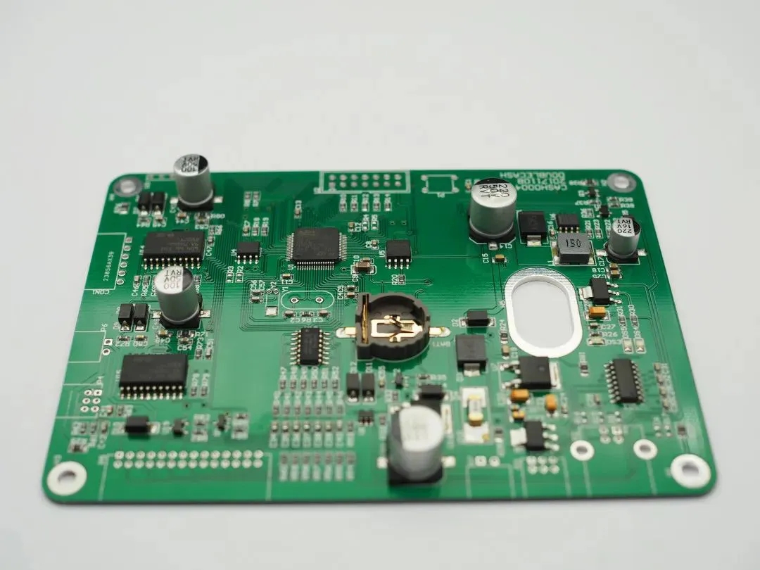
According to the number of layers, PCB can be divided into single panel, double panel, and multi-layer PCB.
First is the single panel. On the most basic PCB, parts are concentrated on one side and wires are concentrated on the other side. Because wires only appear on one side, this PCB is calLED single-sided circuit board. Single panel is usually SIMple to make and low in cost, but its disadvantage is that it cannot be applied to too complex products.
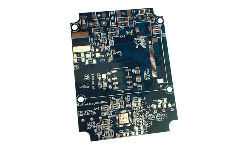
Double panel is an extension of single panel. When single-layer wiring cannot meet the needs of electronIC products, double-sided panel will be used. Both sides are copper coated and wired, and the line between the two layers can be conducted through the via to form the required network connection.
Multilayer board refers to a printed board with more than three conductive graphic layers and insulating materials between them laminated at intervals, and the conductive graphics between them are interconnected as required. multilayer circuit board (MLPCB) is the product of the development of electronic information technology in the direction of high speed, multi-function, large capacity, SMAll volume, thin and lightweight.
PCB can be divided into soft board (FPC), hard board (PCB) and soft hard combination board (FPCB) according to characteristics. These circuit boards have different substrate materials, which are explained below:
PCB manufacturing, PCB design and PCBA processing manufacturers will explain the selection of PCB substrate materials that you must know

1. ElectrolyticNi/Au
2. OSP board (OrganicSolderabilityPreservatives)
3. ImmersionAg
4. ElectrolessNi/Au, ENIG
5. ImmersionTin
6. Tin spraying plate
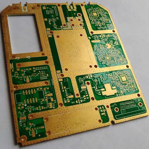
1. Gold plated plate
The cost of the gold-plated plate process is the highest among all the plates, but at present, all the existing plates are the most stable and most suitable for the lead-free process. Especially for some electronic products with high unit price or high reliability, it is recommended to use this plate as the base material.
2. OSP board
The OSP process has the lowest cost and is easy to operate. However, the popularity of this process is still poor because the assembly plant has to modify the equipment and process conditions and the rework is poor. Using this type of plate, after high temperature heating, the protective film pre coated on the PAD is bound to be damaged, resulting in reduced solderability, especially when the substrate is subjected to secondary back welding. Therefore, if the process needs another DIP process, At this time, the DIP end will face welding challenges.
3. Silver plate
Although "silver" itself has a strong mobility, which leads to the occurrence of electric leakage, today's "silver immersion" is not a pure metallic silver in the past, but an "organic silver" co plated with organic matter. Therefore, it has been able to meet the needs of the future lead-free process, and its solderability life is longer than the OSP board.
4. Melting plate
The biggest problem with such substrates is the "BlackPad". Therefore, many large manufacturers do not agree to use the lead-free process, but most domestic manufacturers use this process.
5. Tin melting plate
This kind of substrate is easy to be polluted and scratched. In addition, the process (FLUX) will oxidize and discolor. Most domestic manufacturers do not use this process, so the cost is relatively high.
6. Tin spraying plate
Because of its low cost, good solderability, good reliability and strongest compatibility, this kind of tin spraying plate with good soldering characteristics cannot be used in the lead-free process because it contains lead.
In addition, "tin silver copper tin spraying plate" is difficult to obtain characteristic data because most of them do not use this process
PCB manufacturing, PCB design and PCBA processing manufacturers will explain the choice of PCB substrate materials that you must know.


