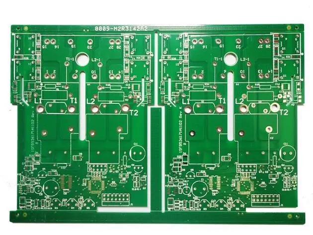
Learn at least a few points about PCB Layout:
(1) For the basIC principle of circuit, please refer to Basics of Circuit Analysis.
(2) Select the design tool and recommend CADence. I have also used AD, and personally feel that Cadence is more powerful and convenient. In addition, you want to take a circuit board with cutting-edge technology. I don't know how to define the cutting-edge. In fact, the most challenging aspect of a PCB is the contradiction between design and cost Fab capabilities. There are dozens of layers of boards (the most 48 layers and the least 24 layers have been made at present), SMAll pin pitches, narrow routing space, strict signal quality requirements, cumbersome routing constraints, and some columns of checks after completion, I believe it will be more convenient and easy to complete these tasks with Cadence.

(3) It is important to be able to use cadence to draw schematic diagrams. If you do not know the circuit principle, it is difficult to make a good placement (I do not know whether this term is universal, so I would like to explain: the actual Layout of components in the schematic diagram on the PCB). I think that a good placement actually completes more than half of a PCB design.
(4) Make good use of the space of PCB according to the schematic diagram, and make reasonable placement to ensure the best signal path and the largest signal wiring space. After placement, adjust the silk, which is the face made by the final board.
(5) Be able to design a reasonable and optimal PCB stackup (without sacrificing the signal quality, take into account the cost and routing complexity, because the more layers, the better the routing, but the higher the cost). Design the routing constraint rules, and then complete the Layout.
(Personally, I think that layout is the SIMplest in the whole process, because under constraint conditions, you can complete the final layout work with a little experience.)
(6) Know the actual fab capabilities of fab manufacturers. Of course, you should know whether your PCB can be made and whether the manufacturer can generate it (if you design 100 layers of boards (even if there is an estimate, it is sky high), I don't know which manufacturer can generate them. I know that the most fab around is 60 layers (40x60cm, more than 10 W dollars), and I haven't heard of 70 layers)
(7) Be able to make quotations and know the charges of each Fab, lamination, blind hole, buried hole, plug hole, back drilling, machining accuracy, drilling ratio requirements, line width, etc. You can estimate the quotation at the beginning of the schematic diagram, and even take the cost into account in the design, so that the final product has competitive price.
(8) After the PCB is completed, it will check the signal, including impedance matching and other long line width checks, power line load capacity checks, repeated routing checks, short circuit and open circuit checks, signal return path checks, and the actual Fab capacity checks, line width checks, line spacing, line hole spacing, and so on.
(9) Generate Fab file and submit it to Fab manufacturer for production.
(10) There is also a missing point above. With regard to the BOM option, according to the schematic diagram, consider the cost and supply cycle of the device, and the impact on the placement (if the resistors are all of the same parameters, in most cases I would like to choose the small size, because it can save PCB space) to choose the most appropriate device.


