ElectronIC manufacturers explain how PCB design can save money?
Does the panel design belong to PCB Layout, board factory or SMT factory? Does Layout care about panel? What does the board factory care about about panel splicing? What is the meaning of panel style to SMT process? When you get a single board Gerber, do you want it to be ABAB or AAAA? Two, four or more? Where, how much, and the length and width of the connecting bridge? What is the difference between ABAB and AAAA boards in placing MARK points and locating holes? What are the requirements for the distance between components and tab connecting bridge? What if there are components protruding from the plate edge? What is the algorithm for panel size and panel utilization This article will work with you to study PCB assembly.
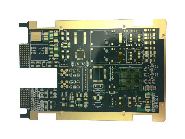
PCB assembly is to combine several PCB unit boards with various possible connection methods, as shown in the following figure. Usually, when designing a PCB, the hardware designer considers the layout of electrical signals and components on the circuit board, and focuses on the function of the product. The manufacturing and assembly of PCB are considered less. To achieve smooth PCB manufacturing, especially in SMT assembly, special attention should be paid to pcb assembly design.
1、 Purpose and significance of panel
To improve the SMT assembly efficiency, the more boards a panel contains, the less the average time for a single PCB to run on the track, and the higher the utilization rate of the mounting equipment, which can greatly improve the SMT production efficiency.
Improve SMT production quality and prevent defective problems in the production process. The distribution density of components on PCB is large. The contour of some components, such as board edge connectors, may exceed the edge of PCB. Before reflow welding or wave soldering is completed, these components are movable. Therefore, additional processes are required to increase the entire PCB panel area to prevent these board edge components from being affected by external factors and reducing the assembly quality.
Easy to operate and prevent damage. The design of panel assembly is also to facilitate the operation of the production line. The assembly of a PCB needs to go through many steps. The finished PCB or sEMI-finished PCB is put into the turnover box, and the turnover rack is used for transfer, storage, storage, transportation, etc. During these operations, specific process edges are required to prevent the components on the PCB from being damaged.
2、 PCB panel design rules
No matter what kind of PCB, it is usually necessary to use the panel structure. However, there are many ways of panel design, and sometimes it is difficult to determine which way to use and the number of panels, which requires comprehensive consideration of various factors.
There are generally two methods for PCB assembly, ABAB or AAAA. It is not easy to say which type of panel is good. This needs to be determined by considering the density and distribution of components on the panel and the equipment configuration. Both types of panel have their advantages and disadvantages.

1. ABAB, commonly known as mandarin duck board, yin and yang board, or front and back panel design, is characterized by symmetrical component distribution on both sides of the panel. The advantages of this design are that the equipment configuration is SIMple and easy, and the preparation operation before production is simple and easy. All SMT assembly needs only one preparation: a steel mesh, a set of patch procedure, SPI inspection procedure, reflow welding temperature curve, etc. However, for products with large difference in component distribution density on both sides of PCB, this may lead to other problems. In some product designs, most of the components may be concentrated on one side of the PCB, while there are only a few simple packaged components on the other side. This ABAB assembly method is not good. This design sometimes leads to printing and mounting problems of some fine pitch components. If there are high quality components on the board, sometimes it will also bring the risk of components falling down during the secondary reflux. Finally, for mass production, the equipment utilization rate will not be too high as a result of such splicing.
2. AAAA/BBBB, a non negative plate design, has the advantage of reasonably arranging equipment configuration and production process according to the distribution characteristics of components on the plate: size and density, and improving equipment utilization. Also, because the components with the same structure are on the same side of the panel, the production process can be reasonably arranged, for example, to avoid the printing short circuit of closely spaced components or the dropping of high profile and large quality components during the secondary reflow. The main disadvantage of this type of panel assembly is that the production and assembly of the two sides of the panel are completely different. Contrary to ABAB, all preparations, such as steel mesh, SPI inspection procedure, mounting procedure, AOI inspection, reflux temperature curve, etc., are different on both sides, and even the production line needs to prepare two, which is not applicable to SMAll batch and multi model products. Of course, for large batches, if the production line configuration is tight, it is not recommended to be the preferred design. Especially in the NPI stage, it brings troubles to the production planning.
3. Sometimes, multiple types of boards are spliced in one panel, which is also possible, as shown in the following figure. If the product contains multiple PCBs and the distribution of signal layers inside these boards is similar, this design can be considered.


