10 precautions for selecting PCB gongs and knives
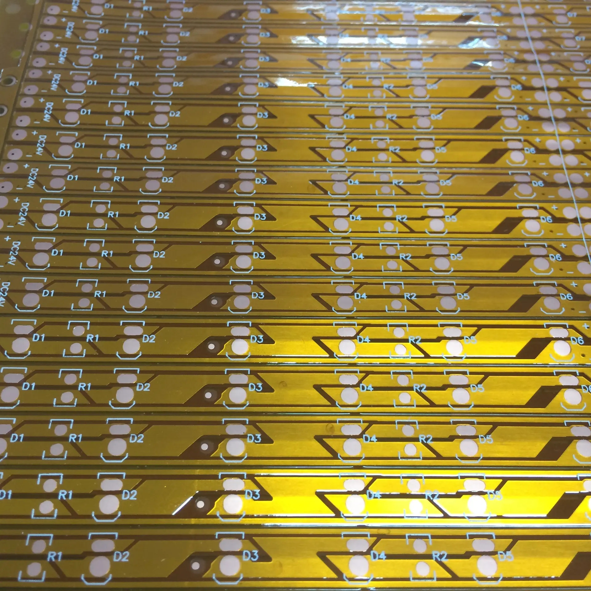
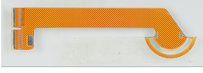
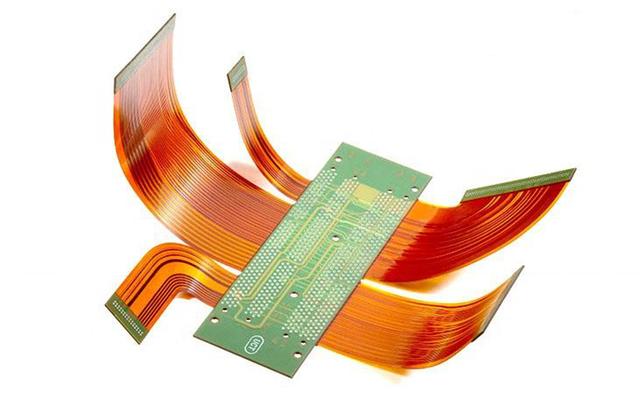
PCB circuit boards are almost used in all electronIC products, from watches and earphones to military and aerOSPace. Although they are widely used, most people do not know how PCB is produced. Next, let's learn about the manufacturing process and production process of PCB!
The PCB manufacturing process can be roughly divided into two parts. Each process requires multiple processes. It should be noted that the process flow of boards with different structures is also different. The following process is the complete manufacturing process of multilayer PCBs;
1、 Inner layer; It is mainly for making the inner circuit of PCB; The production process is:
1. Cutting: cut the PCB substrate to the production size;
2. Pretreatment: clean the surface of PCB substrate and remove surface contaminants
3. Film pressing: paste the dry film on the surface of PCB substrate to prepare for subsequent image transfer;
4. Exposure: use the exposure device to expose the film attached substrate with ultraviolet light, so as to transfer the image of the substrate to the dry film;
5. DE: Develop, etch and remove the exposed substrate, and then complete the fabrication of the inner plate
2、 Internal inspection; It is mainly used to detect and maintain board sub circuits;
1. AOI: AOI optical scanning, which can compare the image of the PCB with the data of the good board that has been recorded, so as to find the notch, depression and other undesirable phenomena on the board image;
2. VRS: The defective image data detected by AOI is sent to VRS for maintenance by relevant personnel.
3. Wire repair: weld the gold wire on the notch or depression to prevent poor electrical property;
3、 Pressing; As the name implies, a plurality of inner plates are pressed into one plate;
1. Browning: Browning can increase the adhesion between board and resin, and increase the wettability of copper surface;
2. Riveting: cut the PP into SMAll sheets and make the inner layer plate match the corresponding PP
3. Overlapping and pressing, target shooting, gongs edge, edge grinding;
4、 Drilling; According to the customer's requirements, holes with different diameters and sizes are drilLED on the boards by using a drilling machine to make holes between boards for subsequent processing of plug-ins, which can also help heat dissipation of boards;
5、 Primary copper; Copper plating is applied to the drilled holes of the outer plate to make the circuit of each layer of the plate conductive;
1. Deburring line: deburr the edges of board holes to prevent poor copper plating;
2. Glue removal line: remove the glue residue in the hole; So as to increase adhesion during micro etching;
3. One copper (pth): copper plating in the hole makes the circuit of each layer of the board conductive and increases the copper thickness;

6、 Outer layer; The outer layer is roughly the same as the first step of the inner layer process, which is intended to facilitate the subsequent process to make lines;
1. Pretreatment: Clean the board surface by pickling, brushing and drying to increase the dry film adhesion;
2. Film pressing: paste the dry film on the surface of PCB substrate to prepare for subsequent image transfer;
3. Exposure: UV light irradiation is carried out to make the dry film on the board form a polymerized and non polymerized state;
4. Development: Dissolve the dry film that has not polymerized during the exposure process, leaving space;
PCB gongs and knives play a very important role in the production process of circuit boards. They affect the drilling accuracy and consistency formed by cutting. In addition to selecting PCB gongs and knives of big brands, it is also necessary to consider economic conditions and select the most appropriate gongs and knives under production conditions.
1. Holes shall be considered.
1) NC machine tools generally do not have jigs for hole processing. Due to the rigidity and poor cutting conditions of PCB gongs, the diameter D of pcb gongs should meet the conditions of L/D ≤ 5 (L is the drilling depth).
2) Before drilling, the central drill shall be used for positioning to ensure the positioning accuracy of hole processing.
3) Floating reamer can be used for fine reaming, and the hole opening shall be chamfered before reaming.
4) When boring, symmetric multi blade boring cutter head shall be selected as far as possible for cutting to balance radial force and reduce boring vibration.
5) Try to choose a thicker and shorter cutter bar to reduce cutting vibration.
2. Milling shall be considered
1) The milling cutter embedded with non regrinding indexable cemented carbide insert is mainly used for milling the plane. The diameter of the pcb milling cutter should be smaller in rough milling and larger in fine milling. When the machining allowance is large and uneven, the cutter diameter should be smaller, otherwise the machining quality of the workpiece will be affected due to the deep cutter MARK.
2) Ball end milling cutter, annular milling cutter, drum milling cutter, tapered milling cutter and disc milling cutter are often used for machining solid surfaces or workpieces with variable bevel profile.
3) High speed steel vertical PCB milling cutter is mainly used for machining boss and groove. If the machining allowance is small and the surface roughness is required to be high, the end milling cutter with cubic boron nitride insert or ceramic insert can be selected.
4) For rough machining of blank surface or hole, the corn milling cutter embedded with hard alloy can be selected for strong cutting.
5) For grooves with high machining accuracy requirements, an end mill with a diameter smaller than the groove width can be selected. First, mill the middle part of the groove, and then use the tool radius compensation function to mill both sides of the groove.
PCB manufacturers often pay little attention to the selection of PCB gongs and knives, which may have a negative impact on quality and cost.


