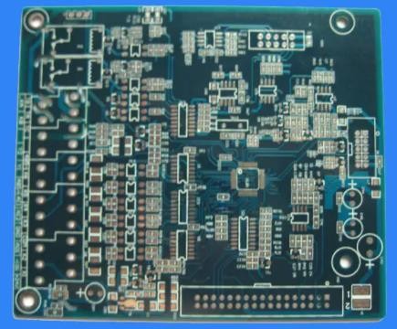
Imperfection and limitation of FPC design process
Poor FPC design for SMT production
The assembly quality of SMT is directly related to the design of FPC, whICh is very important. Flexible circuit board design is the primary condition to ensure the quality of chip assembly. In SMT manufacturing, poor FPC design is very harmful.
1.1. A large number of welding defects are caused.
The FPC pads corresponding to SMD/SMC devices are designed correctly, and there is a SMAll deviation in placement, which is corrected by the tension on the molten tin surface during reflow soldering (SMT is calLED self correction effect); On the contrary, if SMD/SMC, the pad design of FPC corresponding to the equipment is unreasonable or incorrect. Even if the placement position is very accurate, welding defects such as component offset, suspension bridge, tombstone and faulty soldering will occur after reflow soldering.
1.2. Delayed delivery leads to customer dissatisfaction.
circuit board

The workload of repairing and repairing circuit boards was increased, which wasted man hours and delayed the customer's delivery, leading to customer dissatisfaction.
1.3. New process flow, unreasonable use of resources and rework, and new process flow, waste of data and waste of resources. The resources can not be used reasonably.
For rework, the rework process shall be added during the rework process. Rework process
The unreasonable selection of SMD/SMC devices and process data will also lead to the failure and waste of SMD/SMC devices and FPC.
1.4. Damaging SMD/SMC equipment and scrap FPC products after returning to the factory
During the maintenance of installed products, SMD/SMC equipment may be damaged (some SMT equipment cannot be reworked twice) and FPC may be scrapped.
For example, for rework of BGA equipment, the removed equipment must be re balled before reuse. The solder leg of the data cannot be repaired repeatedly, otherwise it is easy to cause the solder leg to fall off (SMT is called cap dropping phenomenon)
1.5. After maintenance, it will directly affect the reliability of products and SMD/SMC equipment.
The welding process requires two to three times of heating, which will greatly reduce the binding force between FPC pad copper and PI, which will directly affect the defects of FPC in the assembly process, and the power efficiency of SMD/SMC devices will also be reduced.
1.6. Unreasonable design will affect placement efficiency and machine utilization.
Due to unreasonable design, the manufacturability of products in the SMT assembly process is poor, which increases the difficulty of placement process and affects placement efficiency and machine utilization.
1.7. Product development time affecting customers
Due to the unreasonable design of SMD/SMC pads, SMD/SMC pads on FPC products must be redesigned and sampled. This will extend the delivery time of FPC products and directly affect the progress of customer assembly and release. It affects the customer's product development time and development cycle.
2. Design of SMD/SMC component pad
2.1. Design equipment to equipment spacing. In production, it is found that the spacing of SMD/SMC pads is too small, which is easy to cause bridging. This, in the design, the spacing between components should be as large as possible, but the high density of component installation limits the spacing between components. It may be too big. Practice has proved that the pad spacing of adjacent components is more than 0.3mm, and there is almost no bridging.
3. Through hole design.
In the pad design of SMD/SMC devices in FPC FPC flexible printed circuit board, it is not allowed to set a through-hole in the pad area, or set the through-hole to be directly connected to the pad to prevent solder loss during heating. Through several design explorations and production practices, it has been proved that the causes of component welding and solder leakage between device pins and pads are caused. When the through-hole is set at a distance of 0.35 mm from the pad, it usually will not lead to faulty soldering or solder skips.
4. Design of bonding pad of SMD/SMC equipment connected to power line and ground wire.
In the design of flexible circuit board, the power line and ground line connected to SMD/SMC gasket should not be wider than 0.2mm to connect the thin neck conductor to prevent the conductor from being too thick to absorb more heat and steal tin, which may lead to faulty soldering, missing component welding or installation, but the thin neck conductor may affect some electrical parameters of the components, This will not affect the connection of power line and ground wire The wires connected to the pad can be designed as two or three narrow neck wires, which are connected to the pads from different directions of the pads


