PCB precautions and electronIC components are damaged
Considerations during fabrICation PCB
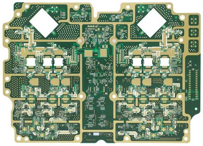
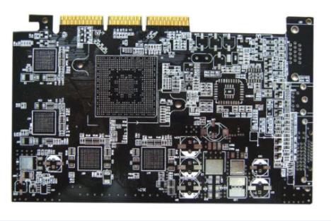
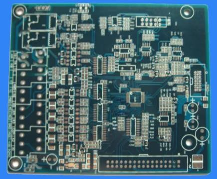
At this stage, in the field of electronic product processing, PCB is indispensable as one of the most important electronic components. At this stage, there are various types of PCB, such as high-frequency PCB, microwave PCB and other types of PCB, which have been recognized in the MARKet. PCB manufacturers have specific production processes for various types of boards. But in general, the following three aspects need to be considered in the production and processing of PCB
1. Consider the selection of substrate
The base materials of PCB can be divided into two categories: organic materials and inorganic materials. Each material has its own unique advantages. In this case, the selection of substrate type takes into account various characteristics, such as dielectric properties, copper foil type, base slot thickness, and production and processing characteristics. Among them, the thickness of the surface copper foil is the key factor affecting the effectiveness of the printed circuit board. Generally, the thinner the thickness is, the more convenient the etching is, and the improvement of the graphic accuracy is beneficial.
2. Consider the setting of production environment
Indoor environment PCB production and processing workshop is also a very important aspect The control of working environment temperature and air relative humidity is a particularly important factor If the temperature of the working environment changes too much, this may cause the hole in the base plate to crack
Circuit board

If the relative humidity of the air is too high, the humidity will adversely affect the performance of the substrate with strong water absorption, mainly in terms of dielectric efficiency Therefore, it is extremely important to maintain appropriate indoor environmental conditions during PCB production and processing
3. Consider the selection of process flow
The production of printed circuit board is easily affected by many factors. Production and processing layers, stamping process, surface coating treatment and other processes will affect the quality of PCB finished products. In this case, the indoor environment of these processes and the production and processing of PCB boards have fully considered the characteristics of production equipment, and can be flexibly adjusted according to the type of PCB boards and production and processing requirements.
To sum up, PCB production and processing need to consider the selection of substrate, the setting of production environment and the selection of process flow. At the same time, the processing and blanking methods of PCB engineering materials also need to be carefully selected, which is closely related to the smoothness of PCB.
Damage Characteristics of Electronic Components in PCB
resistance damage
Resistance is the component with the largest total amount of electrical equipment, but it is not the component with the highest damage rate. Open circuit is the most common type of resistance damage. It is rare for the resistance value to become larger, and it is also rare for the resistance value to become SMAller. Common types include carbon film resistors, metal film resistors, wire wound resistors, and fuse resistors.
The first two resistors are the most widely used. One of the damage characteristics is the high damage rate with low resistance (less than 100 Î) and high resistance (more than 100k Î) Very little damage; Secondly, when low resistance resistors are damaged, they are usually scorched and blackened, which is easier to detect, while high resistance resistors are rarely damaged. Wirewound resistors are usually used for high current limits and have low resistance. When the cylindrical wound resistor is burnt out, some will turn black or the surface will break, while some will have no trace. The cement resistor is a wire wound resistor, which may break when burned out, otherwise there will be no visible trace. When the fuse resistor is burnt out, a piece of skin will be burnt off on the surface, some of which have no trace, but usually will not be burnt out or blackened. According to the above characteristics, we can focus on checking the resistance and quickly find the damaged resistance.
The electrolytic capacitor is damaged
Electrolytic capacitors are widely used in electrical equipment with high failure rate. The electrolytic capacitor is damaged in the following forms: first, the capacity is completely lost or reduced; Second, slight or severe leakage; The third is capacity loss or capacity reduction and leakage. The methods to find damaged electrolytic capacitors are:
(1) Look: Some capacitors will leak when they are damaged, and there will be a layer of oil on the surface of the circuit board under the capacitor or even on the surface of the capacitor. Such capacitors shall not be used again; Some capacitors will expand after being damaged, and such capacitors cannot be used any longer;
(2) Touch: After starting, some electrolytic capacitors with serious leakage will heat up, even when touching with fingers, so this capacitor must be replaced;
(3) There is electrolyte in the electrolytic capacitor. Prolonged baking will cause the electrolyte to dry and reduce capacitance. It is very important to check the capacitors near the radiator and high-power components. The closer they are, the more damage they may cause. The greater the gender.
Damaged semiconductor devices, such as diodes and triodes
The damage of the diode and the triode is usually the breakdown or open circuit of the PN junction, in which the breakdown and short circuit account for the majority. In addition, there are two damage effects: one is that the thermal stability deteriorates, there is no problem during startup, and soft breakdown occurs after a period of operation; The other is the deterioration of the characteristics of the PN junction. In the 1k measurement with the multimeter R *, all the PN junctions are normal, but they cannot work normally after using the computer. If you use R * 10 or R * 1 low range measurement, you will find that the forward resistance of the PN junction is greater than the normal value. The second and third electrodes can be measured on the road with a pointer multimeter. A more accurate method is to set the multimeter to R * 10 or R * 1 (usually R * 10 is used, and then R * 1 is used when it is not obvious). 2. The forward and reverse resistance of the 3-pole tube PN junction. If the forward resistance is not too large (relative to the normal value) and the reverse resistance is large enough (relative to the forward value), the PN junction is normal. Otherwise, it is worth noting. Test after welding. This is because the peripheral resistance of the diode and triode of the circuit usually exceeds hundreds or thousands of ohms. When the low resistance value of multimeter is used to measure on the road, the influence of peripheral resistance on PN junction resistance can be basically ignored.
Damaged IC
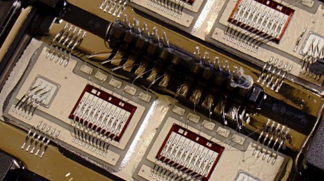
The internal structure PCB integrated circuit is complex and has multiple functions. No part of it can work without problems There are also two types of damage to integrated circuits: complete damage and poor thermal stability When it is completely damaged, you can remove it and compare the forward and reverse resistance of each pin to the ground using the same model of integrated circuit. You can always find one or several pins with abnormal resistance Poor thermal stability. When the equipment is working, you can use absolute alcohol to cool the detected IC If the fault occurs late or does not occur again, it can be determined Usually, this possibility can be ruLED out only by replacing the integrated circuit with a new one


