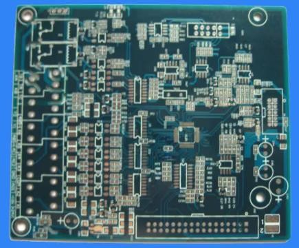
Precautions for PCB drawing and crystal welding
General specifICation PCB drawings
PCB contains four files: schematic diagram, schematic diagram library, package library file, and PCB file
First, create a new PCB project: File ->New ->Project ->PCB project
1. Schematic file name. SchDoc:File->new->Schmatic
2. Schematic library file name. Library: File ->New ->Library ->Schematic Library
3. Package library file name. PCB library: File ->New ->Library ->PCB library
4. PCB file name. PCB file: File ->New ->PCB
PCB common unit
1mil=0.0254mm
100mil=2.54mm
1 inch=1000mil=25.4mm
The typical via sizes used in PCB design and production are as follows:
The size of the via hole used for grounding or other special needs on the PCB is: the hole diameter is 16mil, the pad diameter is 32mil, and the anti pad diameter is 48mil;
The size of through-hole used when the plate density is not high: the hole diameter is 12 mil, the pad diameter is 25 mil, and the reverse pad diameter is 37 mil;
The size of through-hole used when the plate density is high: the hole diameter is 10mil, the pad diameter is 22mil or 20mil, and the reverse pad diameter is 34mil or 32mil;
The size of through-hole used under 0.8mm BGA is: aperture 8mil, pad diameter 18mil, and reverse pad diameter 30mil.
The line spacing is generally not less than 6mil
Circuit board

The distance between copper and copper is usually set at 20mil
The distance between copper sheet and trace, copper sheet and through-hole (via) is usually 10mil
The power cord is generally 30mil
All line widths are generally not less than 6mil
The conventional wiring of the cardboard factory is 8mil, and the processing capacity is: the minimum line width/line spacing is 4mil/4mil. From the perspective of cost, the width of signal line is usually 8mil
The minimum size of the through-hole is 10/18mil, and the other options are 10/20mi or 12/24mil. It is better to use common vias.
All characters should be consistent in the X or Y direction. The size of characters and silk screen should be uniform, generally 6mil and 60mil
Via parasitic capacitance
The via itself has parasitic capacitance to ground. If it is known that the diameter of the isolation hole on the ground plane of the via is D2, the diameter of the via pad is D1, the thickness of the PCB is T, and the dielectric constant of the board substrate is Q µ, then the parasitic capacitance of the via is about C=1.41 Q µ TD1/(D2-D1)
The main effect of via parasitic capacitance on the circuit is to prolong the signal rise time and reduce the circuit speed.
In the design of high-speed digital circuits, the damage caused by via parasitic inductance is often greater than that caused by parasitic capacitance. Its parasitic series inductance will weaken the contribution of bypass capacitors and the filtering effect of the whole power system. We can SIMply use the following formula to calculate the approximate parasitic inductance of the vias: L=5.08h [ln (4h/d)+1], where L is the inductance of the vias, h is the length of the vias, and d is the center diameter of the vias. It can be seen from the formula that the diameter of the through-hole has little influence on the inductance, while the length of the through-hole has the greatest influence on the inductance.
Using the above example, the inductance of the through-hole can be calculated as: L=5.08x0.050 [ln (4x0.050/0.010)+1]=1.015nH. If the rise time of the signal is 1ns, its equivalent impedance is XL=L/T10-90=3.19 Î). When high frequency current passes through, this impedance can no longer be ignored. It should be noted that when connecting the power supply surface and the ground plane, the bypass capacitor needs to pass through two vias, and the parasitic inductance of this vias will increase exponentially.
Precautions for soldered circuit board crystal oscillator
First of all, the soldering temperature of circuit board welding should not be too high, and the soldering time of circuit board welding should not be too long to prevent the internal deformation and instability of crystals. When the crystal case needs to be grounded, ensure that the case and pins are not accidentally connected to cause a short circuit. This crystal will not vibrate. Make sure that the solder joints of the two pins are not connected, otherwise the crystal will stop vibrating. For crystal oscillators to be cut, attention should be paid to the influence of mechanical stress. After the circuit board is welded, it must be cleaned to prevent the insulation resistance from not meeting the requirements.
How to weld the circuit board to the crystal oscillator
First of all, we know that the soldering method of quartz crystal oscillator PCB is related to its packaging. Parts and patches are two different welding methods. Wafer oscillator is divided into manual circuit board welding and automatic circuit board welding. The welding of plug-in crystal oscillator circuit board is not very complicated. First, place the crystal oscillator on the circuit board with tweezers, and melt the solder with a hot air gun.
Manual welding of SMD crystal oscillator is relatively complicated
1. First, add a proper amount of solder on the chisel (flat spade) or knife edge soldering iron head, DIP a fine brush with flux or use a soldering pen to apply a SMAll amount of flux on the pads at both ends, and then plate it on the pads; Hold the chip crystal oscillator with one hand of the tweezers, place it on the pad corresponding to the center, and do not move it after alignment; On the other hand, pick up the soldering iron, heat one of the pads for about 2 seconds, and then remove the soldering iron; Then heat the mat at the other end in the same way for about 2 seconds.
Special note: pay attention to keeping the SMD crystal insulator close to the pad and place it upright to avoid one end of the crystal insulator from lifting or soldering crankcase If the solder on the pad is efficient, you can repair welding with a soldering iron and welding wire in one hand The time is about one second
2. First, plate an appropriate amount of solder on the bonding pad, blow hot air q1an9 with a small nozzle, adjust the temperature to 200 ° C and 300 ° C, and adjust the wind speed to 12 pieces. When the temperature and wind speed are stable, hold it with tweezers in one hand. Place the assembly in the welding position and note. Hold the hot air q1an9 with the other hand, make the nozzle perpendicular to the parts to be removed, with a distance of 1cm~3cm, and heat evenly. After the solder around the crystal oscillator has melted, remove the hot air q1an9, and remove the tweezers after the solder has cooLED.
In order to save money, many factories will use automatic placement machines for automatic placement. Several problems should be paid attention to when welding the circuit board. If the surface crystal is to be welded, it is recommended to use an automatic placement machine as far as possible, because the chip inserted into the quartz crystal oscillator is relatively thin., The volume is relatively small, and it is easier to weld the ceramic crystal oscillator by hand. The quartz crystal oscillator is usually
1. Generally, the temperature of the tip of the soldering iron is controlled at about 300 ℃, and the temperature of the hot air gun is controlled at 200 ℃ and 400 ℃;
2. During the welding process, it is not allowed to directly heat the part above the heel of the crystal oscillator pin to avoid damaging the internal capacitance of the crystal oscillator;
3. It is necessary to use – 0 welding wire 3mm –136; ® 0.5mm; The tip of the soldering iron is always smooth, without hooks and thorns; The tip of the soldering iron shall not contact the pad repeatedly, and the pad shall not be heated repeatedly for a long time Operating temperature of conventional crystal oscillator, it is between - 40 and+85 ° C Heating PCB pad for a long time may exceed the operating temperature range of crystal oscillator, resulting in shortened life of quartz crystal or even damage In order to avoid damaging the resonator, attention should be paid to time control during welding to avoid unstable product efficiency


