What are the advantages and disadvantages of multilayer PCB?
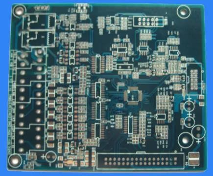
Multilayer PCBA or multilayer printed circuit board is a circuit board composed of two or more conductive layers (copper layers). The copper layer is pressed together by the resin layer (prepreg). Due to the complex manufacturing process, low output and diffICult rework of multilayer PCBA, its price is relatively higher than that of single-layer and double-sided PCBs.
The multilayer pcb circuit board has at least three conductive layers, two of which are on the outer surface, and the remaining one is integrated into the insulating board. The electrical connection between them is usually realized through the plated through-hole on the cross section of the circuit board. Unless otherwise specified, multilayer printed circuit board is the same as double-sided board, which is generally plated through hole board
Advantages and disadvantages of multilayer PCB

advantage:
one
High assembly density
Multilayer PCBs increase their density by layering. This increased density allows for greater functionality, improved capacity and speed, deSPIte the SMAller PCB size.
two
Small size
Multilayer PCB increases the surface area of the circuit board by increasing the number of layers, thereby reducing the overall size. This will allow higher capacity multilayer PCB to be used in smaller devices, while large capacity single PCB must be instalLED in larger products.
three
Light
Multi layer PCBA production can complete the same workload as multiple single-layer boards, but with smaller size, fewer connecting components and lighter weight. This is an important consideration for small Electronic devices that need to consider weight.
The multilayer PCB circuit board has at least three conductive layers, two of which are on the outer surface, and the remaining one is integrated into the insulating board. The electrical connection between them is usually realized through the plated through-hole on the cross section of the circuit board. Unless otherwise specified, multilayer printed circuit board is the same as double-sided board, which is generally plated through hole board
Disadvantages:
one
High cost
The manufacturing process of multilayer PCB is complex and difficult to manufacture, so the cost is relatively high
two
Long manufacturing time
The more layers of boards, the more time-consuming they are and the longer they take to manufacture.
three
Testing methods requiring high reliability.
The more difficult the Multilayer board manufacturing is, the more precise the machine is required to detect to ensure the product quality.
Multilayer printed circuit is the result of the development of electronic technology towards high-speed, multi-function, large capacity and small volume. With the continuous development of electronic technology, especially the extensive and in-depth application of large-scale and ultra large scale integrated circuits, multilayer printed circuits are developing rapidly in the following directions: high-density, high-precision and high-level, small wire holes, blind buried holes, high plate thickness to aperture ratio and other technologies to meet the MARKet demand.


