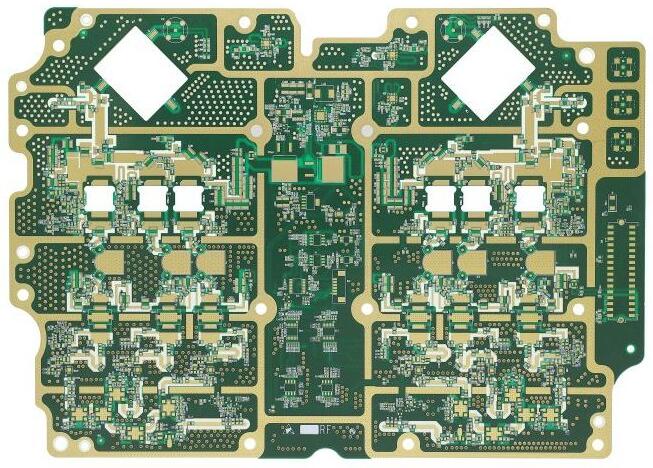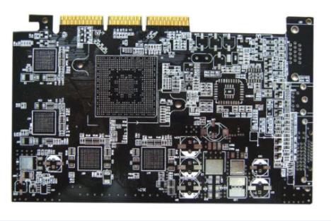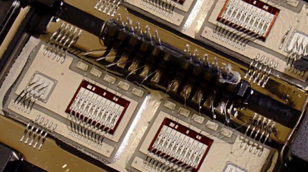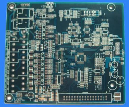
Hot air solver level (HASL) process for PCB
Hot air solver level (HASL) technology is a relatively mature technology at present, but its quality is diffICult to control and stabilize because its process is in a dynamic environment of high temperature and pressure. This paper will introduce some experiences of hot air solver level (HASL) process control.
Hot air spraying layer (HASL) solder coating Hal (usually calLED tin spraying) is a post-treatment process widely used in circuit board factories in recent years. It is actually a process of coating eutectic solder in the metallized hole of printed board and printed wire by combining immersion welding and hot air solver leveling (HASL). The process is to immerse the solder on the printed circuit board, then immerse it in the molten solder, and then pass between two air knives. Use the hot compressed air in the air knife to blow off the excess solder on the printed circuit board, and at the same time remove the excess solder in the metal hole to obtain a bright, flat and uniform solder coating.
The most outstanding advantages of the hot air solder layer (HASL) are that the coating composition remains unchanged, the edges of the printed circuit board can be completely protected, and the coating thickness can be controlled through the air knife; The coating and the base copper are bonded with each other, with good wettability, weldability and corrosion resistance. As the next process of PCB, its quality directly affects the appearance, corrosion resistance and user welding quality of PCB. How to control the process is a concern of circuit board manufacturers. Next, let's talk about some experiences in controlling its process control at the most widely used vertical hot air solver level (HASL).
Printed circuit board

Selection and Application of Flux
The flux used in the Hot Air Solver Level (HASL) is a special flux. Its function in the hot air solver level (HASL) is to start the exposed copper surface on the PCB and improve the wettability of solder on the copper surface; Ensure that the laminate surface is not overheated, protect the solder during cooling after leveling, prevent solder oxidation, prevent solder adhesion to the solder mask, and prevent solder bridging between pads; The waste flux can clean the solder surface, and the oxidized solder is discharged with the waste flux.
The special flux (HASL) at the hot air solver level must have the following characteristics:
1. Must be water-soluble flux, biodegradable and non-toxic.
Water soluble flux is easy to clean, with less residue on the board surface, and will not form ion pollution on the board surface; Biodegradable materials can be discharged without special treatment, which meets the environmental requirements and greatly reduces the harm to human body.
2. Good mobility
As for the activity, that is, to remove the oxide layer on the copper surface and improve the wettability of solder on the copper surface, an activator is usually added to the solder. In the selection, good activity and minimum corrosion to copper shall be considered to reduce the solubility of copper in solder and reduce the damage of smoke to equipment.
The activity of flux is mainly reflected in the loading capacity of tin. Due to the different active substances used in various fluxes, their activities are also different. High active flux, good tin on compact pads, patches, etc; On the contrary, the copper plate surface is prone to copper exposure, and the activity of active substances is also reflected in the brightness and flatness of the tin surface.
3. Thermal stability
Protect green oil and substrate from high temperature impact.
4. Must have a certain viscosity
Hot air solder level (HASL) requires a certain viscosity of the flux, which determines the fluidity of the flux. In order to completely protect the surface of solder and laminate, the flux must have a certain viscosity. Low viscosity flux is easy to adhere to the laminate surface (also known as tin hanging), and easy to bridge in dense locations such as IC.
5. Suitable acidity
The soldering flux with high acidity is easy to peel off the edge of the solder mask before spraying, and the residual flux after spraying for a long time is easy to blacken and oxidize the tin surface. The pH value of general flux is 2.5-3.5, about 5.
Other effects are mainly reflected in the impact on operators and operating costs, such as bad SMEll, high volatile substances, large smoke, tissue coating area, etc. The manufacturer shall make the selection on the basis of experiments.
During the test, the following performances can be tested and compared one by one:
1. Whether the flatness, brightness and holes are blocked
2. Activity: Select the fine density SMD circuit board and test its tin carrying capacity.
3. The circuit board shall be coated with flux for 30 minutes. After cleaning, the peeling of raw oil shall be tested with adhesive tape.
4. Place the spray plate for 30 minutes, and test whether the tin surface turns black.
5. Residues after cleaning
6. Whether dense IC bits are connected.
7. Whether tin is hung on the back of veneer (fiberglass board, etc.).
8. Smoke
9. Volatility, odor size, need to add thinner
10. Whether there is foam during cleaning.
Control and Selection of Process Parameters for Hot Air Solver Leveling (HASL)
HASL process parameters include welding temperature, immersion time, air knife pressure, air knife temperature, air knife angle, air knife spacing and PCB rising speed. The influence of these process parameters on PCB quality will be discussed below.
1. Tin DIPping time:
Tin dipping time is closely related to the quality of solder coating. During immersion welding, the base copper and tin in the solder form a layer of metal compound in IMC and a layer of solder coating on the conductor. The above process usually takes 2-4 seconds, during which good intermetallic compounds can be formed. The longer the time, the thicker the solder. However, if the time is too long, the substrate of the PCB will delaminate and the green oil will bubble. If the time is too short, it is easy to produce sEMI immersion, which will lead to local tin surface whitening and tin surface roughness.
2. Bath temperature:
Lead 37/tin 63 alloy with a melting point of 183 ℃ is the commonly used solder for soldering temperature of printed boards and electronIC components. When the solder temperature is 183 ℃ - 221 ℃, the ability to form intermetallic compounds with copper is very SMAll. At 221 ° C, the solder enters the wetting zone, ranging from 221 ° C to 293 ° C. Considering that the plate is easy to be damaged under high temperature, the welding temperature should be low. It is found that 232 ℃ is the most suitable welding temperature in theory, and 250 ℃ can be set as the best temperature in practice.
3. Air knife pressure:
There is too much solder on the printed circuit board after immersion welding, and almost all the metallized holes are blocked by solder. The function of the air knife is to blow off excess solder and guide the metallized hole without reducing the diameter of the metallized hole too much. The energy used to achieve this is provided by the pressure and flow rate of the air knife. The higher the pressure, the faster the flow rate, and the thinner the solder coating. Recall that blade pressure is one of the most important parameters of the hot air solver level (HASL). Air knife pressure is generally 0.3-0.5mpa
The pressure before and after the air knife is generally controlled to be large in the front and small in the rear, and the differential pressure is 0.05Mpa. According to the distribution of geometric figures on the board surface, the pressure of the front and rear air knives can be adjusted appropriately to ensure that the IC position is flat and the patch is free of protrusions. See the factory manual of our tin spraying machine for specific values.
4. Air knife temperature:
The hot air from the air knife has little effect on the PCB and air pressure. However, increasing the temperature in the air knife helps to expand the air. In this case, when the pressure is constant, increasing the air temperature can provide greater air volume and faster flow rate, thus generating greater leveling force. The temperature of air knife has a certain influence on the appearance of solder coating after leveling. When the air knife temperature is lower than 93 ℃, the coating surface will become dark. With the increase of air temperature, the dark coating tends to decrease. At 176 degrees Celsius, the black appearance disappears completely. The minimum temperature of the air knife shall not be lower than 176 ℃. Generally speaking, in order to obtain good tin surface flatness, the temperature of the air knife can be controlled between 300 ℃ and 400 ℃.
5. Blade spacing:
When the hot air in the blade leaves the nozzle, the flow rate slows down, and the degree of slowing down is proportional to the square of the blade spacing. In this case, the larger the spacing is, the smaller the wind speed is, and the lower the leveling force is. The air knife spacing is generally 0.95-1.25cm. The distance between air knives should not be too small, otherwise air will cause friction on the printed board, which is detrimental to the surface of the printed board. The distance between the upper and lower blades is usually kept at about 4mm, which is too large and easy to cause solder splash.
6. Blade angle:
The angle of the air knife blowing the plate will affect the thickness of the solder coating. If the angle is not adjusted properly, the solder thickness on both sides of the PCB will be different, which may also cause molten solder splash and noise. The angle of most front and rear air knives is adjusted downward to 4 degrees, which is slightly adjusted according to the specific plate type and the geometric distribution angle of the plate surface.
7. PCB rising speed:
Another variable related to the hot air solver level (HASL) is the passing speed between the blades, that is, the rising speed of the conveyor, which affects the solder thickness. The speed is very slow, there is more air blowing on the printed board, and the solder is very thin. On the contrary, the solder is too thick and even blocks the hole.
8. Preheating temperature and time:
The purpose of preheating is to improve the activity of flux and reduce thermal shock. Generally, the preheating temperature is 343 ℃. When preheating for 15 seconds, the surface temperature of the printed board can reach about 80 ℃. Some hot air solver levels (HASL) do not have a warm-up process.
HASL PCB
HASL PCB
Uniformity of solder coating thickness
The solder thickness applied to the hot air solver level (HASL) is basically uniform. However, with the change of geometric factors of the printing line, the leveling effect of the air knife on the solder will also change, and the solder coating thickness at the hot air solver level (HASL) will also change. Generally, the printed wire parallel to the leveling direction has small resistance to air, large leveling force and thin coating. The printed wire perpendicular to the leveling direction has a large resistance to air and a small leveling effect. The coating is thick, and the solder coating in the metallized hole is uneven. Since the solder is in a dynamic environment of high pressure and high temperature as soon as it is taken out of the high-temperature tin furnace, it is difficult to obtain a completely uniform and flat tin surface. However, it can be as flat as possible through parameter adjustment.
1. Select active flux and solder
Flux is the main factor affecting tin surface smoothness. A relatively flat, bright and complete tin surface can be obtained by using a good active flux.
Solder shall be made of high-purity lead tin alloy, and float copper treatment shall be carried out regularly to ensure its copper content is less than 0.03%. For more information, see Workload and Test Results.
2. Equipment adjustment
Air knife is the direct factor to adjust the flatness of tin surface. The angle of the air knife, the change of the pressure and differential pressure of the front and rear air knives, the temperature of the air knife, the distance between the air knives (vertical distance, horizontal distance) and the lifting speed will have a great impact on the surface of the plate. The parameter values are different for different plate types. Some technologically advanced tin spraying machines are equipped with microcomputers, which store the parameters of various sheet types in computers for automatic adjustment.
Clean the air knife and guide rail regularly. The clearance residues of the air knife should be cleaned every two hours. When the output is large, the cleaning density shall be increased.
3. Pretreatment
Micro etching treatment also has a great influence on the flatness of tin surface. If the micro etching depth is too low, it is difficult for copper and tin to form copper tin compounds on the surface, resulting in local tin surface roughness; The poor stabilizer in the micro etching solution will cause the copper etching speed to be too fast and uneven, resulting in uneven tin surface. APS system is generally recommended.
For some types of steel plates, it is sometimes necessary to pretreat the baking tray, which will also have an impact on tin leveling.
4. Pre process control
As the hot air solver level (HASL) is the last treatment, many previous processes will have a certain impact on it, such as poor tin load due to unclean development. Strengthening the control of the previous process can greatly reduce the problems in the hot air solver level (HASL).
Although the solder coating thickness of the above hot air solver level (HASL) is uneven, it can meet the requirements of mil-std-275d.
The above is the explanation given by the editor of pcb circuit board company.
If you want to know more about PCBA, you can go to our company's home page to learn about it.
In addition, our company also sells various circuit boards,
High Frequency Circuit Board and SMT chip are waiting for your presence again.


