Defects of PCB Pattern Copper Plating and Their Elimination
With the increasingly fierce competition in the industry, manufacturers of printed circuit boards continue to reduce costs, improve product quality, pursue zero defects, and win with high quality and low prICe
1. Defect features and causes
2.1 Coating pitting
PockMARKs appears on the patterned partner electing, which is more prominent in the board of directors After the lead and tin are selected, the copper surface is uneven and the appearance is not good After the brush plate is cleaned, the surface pitting still exists, but it is basically smooth, not as obvious as after removing the tin After this phenomenon, the problem of copper electroplating solution CAMe to mind first, because the solution was treated with activated carbon the day before the failure The steps are as follows:
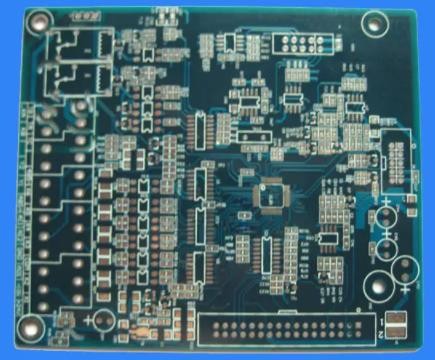
Printed circuit board

1) Add 2 liters of H2O2 under stirring conditions;
2) After fully stirring, transfer the solution to the standby tank, add 4kg of fine activated carbon powder, then add air and stir for 2h, then turn off the stirring to let the solution precipitate The investigation found that the production line transferred the solution from the standby tank to the working tank that night in consideration of the express plan of the next day While transferring solution without circulating filter pump (slow) directly returns from the output of the working tank (coal pipe, fast) Since the off duty time has passed since the solution was transferred back to the working tank, the electroplating personnel did not carry out low current density empty plating on the anode Due to the urgency of the schedule, electroplating personnel did not operate according to the procedure of the process file, and the solution was not completely recycLED and filtered, resulting in mechanical impurities in the solution affecting the coating quality Another factor is that after the phOSPhor copper anode is cleaned, it can't work directly through electrolytic treatment, and there is no time to form a black and uniform "phosphorus film" on the anode surface, leading to the accumulation of a large amount of copper, and Cu+hydrogen to produce copper powder, resulting in coarse and concave coating The dissolution of copper is limited by the control steps, and Cu+cannot be rapidly oxidized to Cu2+ However, the anodic film did not form and Cu-e reaction occurred Cu2+continues to proceed in a fast manipulator, resulting in copper accumulation++, while Cu+is unstable, and is disproportionated by disproportionation Reaction: 2Cu++ Cu2+Cu is deposited on the coating by electrophoresis during electroplating, which affects the coating quality The anodic film formed after low current electrolytic treatment of the anode can effectively control the dissolution rate of copper. Moreover, the anode current efficiency is close to the cathode current efficiency, and the copper ions in the plating solution are kept in balance, preventing the generation of Cu+and maintaining the normal operation of the plating solution The defects of copper electroplating this time also exposed some problems: due to the time relationship, operators sometimes neglect the production process, working time and output, which will affect the quality of products Therefore, the production operation should be carried out in strict accordance with the process file. The production task is tight and the cycle is short. Illegal work should not be carried out Otherwise, the product will be reworked or scrapped due to quality problems, which will affect the product qualification rate, thus affecting the production cycle and reducing the credibility
Troubleshooting: After finding out the cause, replace the pattern copper plating solution filter element to strengthen filtering; In addition, an experimental board 500mm * 500mm is prepared to electrize the anodes of the 6 electrifying tanks specially In this way, the PCB produced the next day was completely normal, except for the electroplating pitting defect of the allegro
1.2 Coating bloom (dendritic)
The surface of the patterned copper electroplating is flower, especially on a large area of coating, which is like a branch, long and short However, the electroplating area is SMAll, and after the PCB board is electroplated on the same day, there are almost no defects in the pads or thin wires to be electroplated. Therefore, the initial halo phenomenon of the coating has not attracted enough attention, and the betrayal is an accidental factor: PCB board, matrix problems, or brushing marks from the pumice plasterer before the pattern transfer after hole metallization Later, with the increase of output, the number of PCB surface flowers became more and more, especially for PCB with drawing number MON_ 1. The size is 265mm * 290mm. The surface area of electroplating area A is 2.35dm2, and the surface area of electroplating area B is 4.48 dm2. Almost half of the PCB surface needs copper plating, so the pattern halo phenomenon is clear at a glance, which seriously affects the appearance of the printed circuit board It is necessary to analyze the characteristics of a large number of defective PCB boards, find out the causes and completely eliminate the faults In order to meet customer satisfaction, the quality department of our center will stop all PCB boards from coating defects: whether there is large-area coating halo or filiform traces on the lines Quality is the life of an enterprise Our technical department will explore the problems of the coating:
1) First of all, according to previous experience, it is judged that the weak corrosion pretreatment solution of pattern electroplating pretreatment contains a large amount of organic matter Because the spraying and cleaning after degreasing may not be enough, the organics in the degreasing solution are taken to the working tank behind and selected as secondary pollution. The adsorption of organics on the pattern to be plated on the PCB surface will affect the adsorption on the cathode This affects the appearance of the coating Therefore, the weak corrosion and prepreg liquid were reopened, which reduced the printing defects in production, but the halo on the PCB surface did not completely disappear In this troubleshooting, it seems that the previous experience did not fully play a role, and then the focus shifted: Is there a problem with oil removal? It is caused by aging of degreasing liquid and unclean degreasing liquid? Check whether the temperature and composition are within the normal range In order to find out the root cause of the defect as soon as possible, the Hall cell test was carried out: a small piece of copper sheet was mechanically brushed with charcoal, and then it was cleaned as cathode electroplating Because the sample is not degreased, but mechanical degreasing still exists. It can be seen that degreasing is not the culprit of this failure
2) After troubleshooting in the small experiment, add CL - and brightener FDT-1 into the working tank in proportion. After full air stirring and loop filtration, wipe the two bar coupler plates of 350mm * 350mm size and then remove the oil? clean? Weak corrosion? clean? Pickling? This pattern is copper plated. After the normal dwell process, the pattern is plated without any defects In this case, the production line continued to run, and the plated PCB was completely normal the next day It can be seen that there are many reasons for coating halo: degreasing solution, weak corrosion solution, prepreg solution, chloride concentration in pattern copper plating solution and brightener FDT-1 will affect the coating quality The inaccuracy of chloride concentration analysis directly affects the adjustment of solution; The addition standard of whitening agent FDT-1 "measuring conductivity of electroplating bath by current integration" can no longer be used The addition of daily whitening agent FDT-1 is mainly combined with Hall cell Experiment and adjust according to the workload of a day Only under the synergistic action of chloride ions and additives, can an ideal coating be obtained Strictly controlling process parameters is the key to produce qualified products, otherwise any out of control parameters will lead to coating defects
1.3 Hydrosphere traces on the coating
There are a lot of water circles on the electroplated copper of the printed circuit board pattern with larger size, especially the water circle around the hole
1) This phenomenon first led our thinking to water spray. Because the spray water circuit of pattern plating line and hole metallization line share a set of water circuit system, the solenoid valve of a single spray pipe fails, and water can only be sprayed continuously In this way, when two lines work at the same time and need to spray at the same time, insufficient pressure will directly affect the spray effect In this case, the double-sided 3-pole printed circuit board was tested. It was produced according to the normal procedure. In addition to connecting the water pipe during spraying to strengthen water flushing, the water loop still exists after the pattern is copper plated From the analysis of defect characteristics, the defects on the surface of electroplated copper are consistent with the traces of water drops It should be a problem of washing However, this has nothing to do with the washing of the pattern plating line Is it due to poor development and cleaning after pattern transfer?
2) Trace back to the source and find the waterway of the graphic transfer. It turns out that a new electrogenerated exposure machine purchased by our center uses a water loop cooling pipe, and its water channel and the cleaning section of the developer use the same water channel When the exposure machine and the developer work at the same time, the spray pressure of the cleaning section of the developer is small; And the PCB board is very large, especially the water sprayed from above is easy to accumulate on the PCB board surface on the ground, which is unfavorable to the circulation of solution In this way, the residual liquid of dry film or wet film development of photoresist is not completely washed After the drying section, the watermark of the mucous membrane is not easy to be found in the subsequent repair work (unlike the residual glue with objective blue film); It is not easy to remove the pattern before electroplating. One hour after copper plating, the mark of the watermark is clear and discernible, with a certain depth, which is not easy to polish and affects the surface appearance of PCB To confirm this conclusion, 10 printed circuit boards with 460mm * 420mm drawing number Y005 were transferred and developed, 5 pieces were directly sent to the pattern electroplating line after air drying, and the remaining 5 pieces were sent to the cleaning machine for cleaning without drying The last step is the pattern plating line After the same pre-treatment and copper plating comparison, it was not found that the printed circuit board with water ring was cleaned on Highway 5, while the printed circuit board was directly sent to the pattern electroplating line, and the water loop could be clearly seen
3) Troubleshooting: Transform the water circuit of the exposure machine so that it is separated from the water washing section of the developing machine; In addition, three rows of upper and lower spray pipes are added after the water washing section of the developer Also, replace the missing and deactivated spray bar on the pattern plating line After repair and transformation, the pattern of electroplated copper is of good quality


