Wiring design of EMC Multilayer PCB board
It is very important to consider the electronIC compatibility (EMC) design in the circuit design stage Take 12 layer board as an example, layered method, wiring rules, ground and power line layout, electromagnetic compatibility Electromagnetic compatibility is a new and comprehensive subject, which mainly studies electromagnetic interference and anti-interference Electromagnetic compatibility means that under the specified electromagnetic environment level, the performance indicators of electronic equipment or systems will not be reduced due to electromagnetic interference, and the electromagnetic radiation generated by them will not exceed the limit level, which will not affect the normal operation of other systems And achieve the goal of non interference between equipment, system and system, common and reliable work Electromagnetic interference (EMI) is caused by the electromagnetic interference source transferring energy to the sensitive system through the coupling path. It includes three basic forms: conductor conduction and common grounding, space radiation or near-field coupling Practice has proved that even if the circuit schematic diagram is correctly designed and the printed circuit board is improperly designed, it will adversely affect the reliability of electronic equipment Therefore, ensuring the electromagnetic compatibility of PCB is the key to the whole system design This paper mainly discusses electromagnetic compatibility Technology and its application in multilayer design Printed circuit board
Printed circuit board

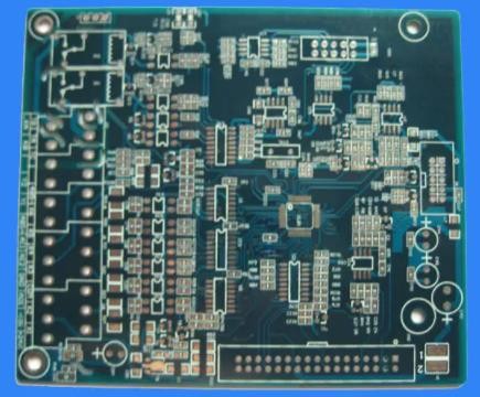
This PCB is the support of circuit components and devices in electronic products It provides the power connection between circuit components and equipment, and is the basic component of various electronic equipment Nowadays, VLSI and VLSI have been widely used in electronic equipment, and the installation density of components is getting higher and higher, and the signal transmission rate is getting faster and faster EMC problems are becoming more and more prominent PCB boards are divided into single sided (single layer boards), double sided (double layer boards) and Multi layer boards Single sided and double-sided circuit boards are commonly used for low density and medium density wiring circuits and circuits with low integration. multilayer circuit boards use high-density wiring and circuits with high integration From the perspective of electromagnetic compatibility, single-sided and double-sided circuits are not suitable for high-speed circuits, and single-sided and double-sided wiring can no longer meet the requirements of high-performance circuits. The development of multi-layer wiring circuits has made it possible to solve the above problems The application is more and more extensive
1. Characteristics of multi-layer wiring
The PCB board is composed of organic and inorganic dielectric materials with multilayer structure The connection between layers is realized by via, and the electrical signal transmission between layers can be realized by electroplating or filling the via with metal materials The reason why multi-layer wiring is widely used has the following characteristics:
(1) There are special power supply layer and ground wire layer inside the multi-layer board. The power layer can be used as noise loop to reduce interference; At the same time, the power layer also provides circuits for all signals of the system to eliminate common impedance coupling interference The impedance of the power line is reduced, thereby reducing common impedance interference
(2) The multi layer board adapters a special ground layer Characteristics of signal line: stable impedance, easy to match, and reduce waveform distortion caused by reflection; At the same time, use special grounding wire The line layer adds distributed capacitance between signal line and ground wire to reduce crosstalk,
2. Composite laminate design PCB
2.1. Cable wiring rules PCB board
The electromagnetic compatibility analysis of multilayer circuit board can be based on Kirchhoff's law and Faraday's law of electromagnetic induction According to Kirchhoff's law, any time-domain signal transmission from the source to the load must have an impedance path Where multiple layers are used for direct current (DC) power or ground reference planes These planes are usually solid planes without any division, because there are enough layers that can be used as power or ground planes. Therefore, it is not necessary to apply different DC voltages on the same layer This layer will serve as the current return path for signals on adjacent transmission lines Creating low impedance current loops is an important EMC goal for these planar layers The signal layers are distributed between the physical reference plane layers. They can be symmetrical striplines or asymmetrical striplines The structure and layout of a 12 - ply plate are illustrated Its hierarchical structure is T-P-S-P-S-S-S-S-S-S-S-S-P-B. "T" is the top layer, "P" is the reference plane layer, "S" is the signal layer, and "B" is the bottom layer From the top to the bottom are the first, second and twelfth floors The top and bottom layers are used as gaskets for components. The signal transmission time at the top and bottom layers should not be too long to reduce the direct radiation of traces Incompatible signal lines shall be isolated from each other in order to avoid mutual coupling interference High frequency and low frequency, large current and SMAll current, digital and analog signal lines are incompatible In the component layout, incompatible components should be placed at different positions on the printed board, and the signal line layout is still necessary Be careful to isolate them During design, pay attention to the following 3 issues:
(1) Determine which reference plane layer will contain multiple power regions for different DC voltages. Assuming that there are multiple DC voltages on the 11th layer, this means that the designer must keep the high-speed signal as far away from the 10th layer and the bottom layer as possible, because the return current cannot flow through the reference plane above the 10th layer, and the capacitors need to be stitched. The 3rd, 5th, 7th and 9th are the signal layers of high-speed signal, respectively The traces of important signals should be routed along one direction as far as possible to optimize the possible number of traces on the layer The signal tracks distributed on different layers should be perpendicular to each other, which can reduce the coupling interference of electric and magnetic fields between lines Layers 3 and 7 can be set as "things" tracks, while layers 5 and 9 can be set as "things" tracks The "North South" route The layer to which the trace is routed depends on the direction of its destination
(2) Layer changes when routing high speed signals, which layer is used for independent wiring to ensure that the return current flows from a reference plane to the required new reference plane This is to reduce the area of the signal loop and the differential mode current radiation and common mode current radiation of the loop The loop radiation is proportional to the current intensity and loop area In fact, the design does not require reflux to change the reference plane, but only from one side of the reference plane to the other For example, the combination of signal layers can be used as a pair of signal layers: the third and fifth layers, the fifth and seventh layers, the seventh and ninth layers, which makes it possible to form a wiring combination in the east-west and north-south directions However, the combination of layer 3 and layer 9 should not be used, because it requires the return current to flow from layer 4 to layer 8 Although decoupling capacitors can be placed near through holes, capacitors become useless at high frequencies due to the presence of lead and over inductance This connection will increase the area of the signal loop, which is not conducive to reducing current radiation
(3) Select the DC voltage for the reference plane layer. In this example, there is a lot of noise on the power supply/due to the high signal processing speed inside the processor, this grounding reference pin is recommended Therefore, it is very important to use decoupling capacitors to provide the same DC voltage to the processor, and use decoupling capacitors as effectively as possible The way to reduce the inductance of these components is to make the connection path as short and wide as possible, and make the through-hole as short and thick as possible If the second layer is designated as "ground" and the fourth layer is designated as the power supply of the processor, the distance between the via and the top layer where the processor and decoupling capacitor are placed should be as short as possible The remaining gap extending to the bottom layer of the circuit board does not contain any significant current and has no antenna effect for a short distance
2.2 The 20-H Rule and the 3-W Rule
In the electronic compatibility design of multi layer PCB, there are two basic principles to determine the distance between the power layer and the edge of the Multilayer board and to calculate the distance between the printing strips: 20-H rule and 3-W rule 20 hour principle: due to the connection between magnetic fluxes, RF current usually exists at the edge of the power plane This coupling between layers is calLED edge effect When high-speed digital logic and clock signal are used, the dynamic surface will interact Coupling RF current The physical size of the power plane should be at least 20H smaller than the physical size close to the ground plane (H is the distance between the power plane and the ground plane) About 10% of the magnetic flux is blocked. If you want to reach 98% of the magnetic flux is blocked, you need a 100% boundary value The 20-H rule determines the physical distance between the power plane and the nearest ground plane, including copper thickness, prefill, and insulating barriers The resonant frequency of PCB itself can be added after 20 hours of use
RF edge effect PCB board s
3-W rule: When the distance between the two printed lines is small, electromagnetic crosstalk will occur between the two lines, which will lead to related circuit failure In order to avoid such interference, the distance between any lines shall be no less than 3 times Line width is not less than 3W (W is the width of printed lines) The printing line width depends on the line impedance requirements. Too wide will affect the wiring density, and too narrow will affect the integrity and strength of the signal transmitted to the terminal Clock circuit wiring, differential pair and I/O port are the basic application objects of 3-W principle The 3-W principle only represents the electromagnetic flux line boundary with 70% crosstalk energy attenuation If the requirements are higher, such as the boundary line of electromagnetic flux, to ensure that the crosstalk energy attenuation is 98%, a 10W interval must be used
2.3 Layout of the ground wire
First of all, establish the concept of distributed parameters. Any metal wire beyond a certain frequency should be regarded as a device consisting of resistance and inductance Therefore, the grounding wire has a certain impedance to form a power circuit. Whether it is single point grounding or multi-point grounding, it must form a low impedance circuit in the actual grounding or rack A typical track 25 mm long will show an inductance of about 15 to 20 mA, and the presence of distributed capacitance will form a resonant circuit between the ground plane and the equipment rack Second, when the grounding current flows through the grounding wire, transmission line effect and antenna effect appear When the line length is 1 hour/4 wavelength, it shows high impedance. The ground wire is actually open. The ground wire becomes an antenna radiating outward. The ground plate is full of high-frequency current and eddy currents formed by disturbances Therefore, many loops are formed between grounding points, and the diameter of these loops (or ground point spacing) should be less than 1/20 of frequency and wavelength. Choosing the right device is an important factor for successful design. Especially when choosing logic devices, try to choose logic devices with a rise time greater than 5ns, and do not choose logic devices whose timing is faster than the circuit requirements
The above is the explanation given by the editor of pcb circuit board company.
If you want to know more about PCBA, you can go to our company's home page to learn about it.
In addition, our company also sells various circuit boards,
High Frequency Circuit Board and SMT chip are waiting for your presence again.


