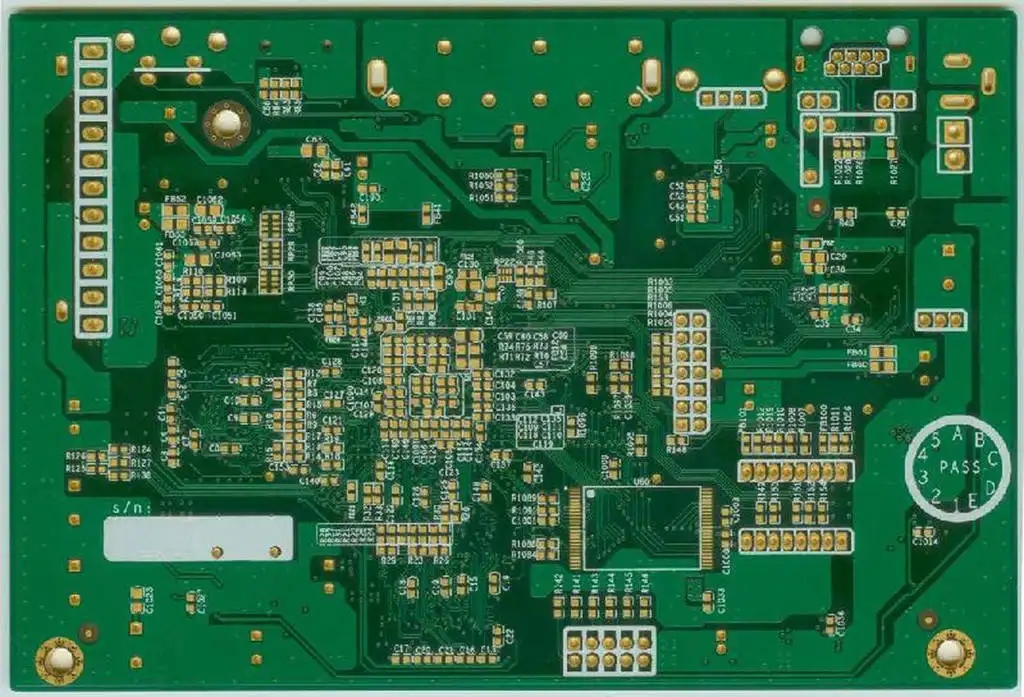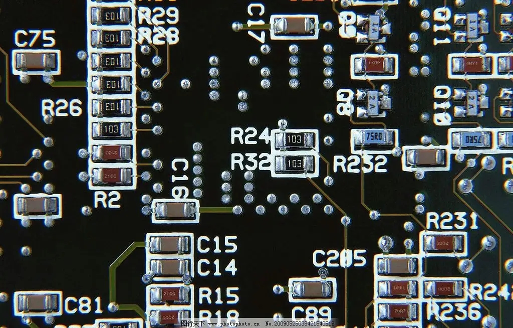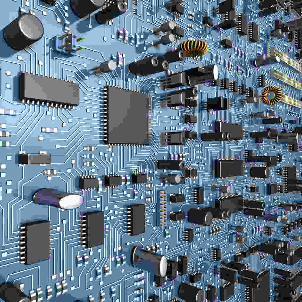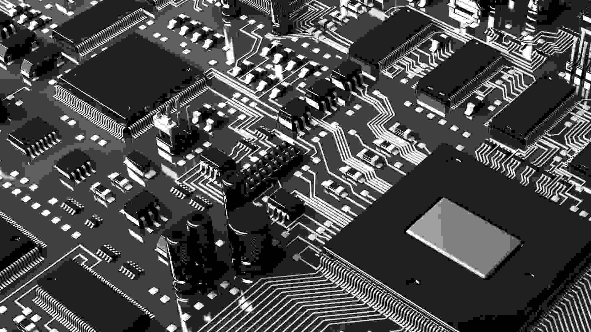
Single-sided, double-sided and multilayer are the three main types of PCB (printed circuit board). Several separate stages are deployed during PCB assembly. All of these people need to operate as teams to produce a holistIC integration process. Each phase needs to move on to the next, and feedback after the final phase is necessary to maintain quality. This way, any problems can be quickly identified and necessary adjustments made. This is an overview of the PCB assembly process.

1. The solder paste
Solder paste must be added in the necessary areas before any components are added to the board. Some of these areas include component pads where solder is added using solder mesh. Solder paste is in the form of tiny solder particles with flux. Add this mixture in place in a manner SIMilar to a typical printing process.
By moving the runner across the screen, the solder paste will penetrate through the screen holes and deposit on the pcb board. Note that only solder deposits were found in the pads. This is because the printed circuit board file is used to generate the welding screen. Therefore, the solder screen is always aligned with the pad. For optimal PCB fabrication results, the amount of solder needs to be monitored to get the correct volume into the resulting joints.
2. Take put
During this part of the PCB manufacturing and assembly process, the board will undergo a process calLED mount. The replacer removes the components from the dispenser and places them in the desired position on the board. The tension in the solder paste helps keep all components in the correct position without shaking the PCB. In order to secure components to the board, certain patches will add glue drops during PCB manufacturing. To avoid maintenance trouble, it is best to use degradable adhesive during welding.
3.The welding
Now that the necessary components are on the PCB, it's time to run the board through the welding machine. Although not common today, some PCB manufacturing processes involve passing the board through a crest welder. Wave soldering does not require adding solder paste to the plate because the machine has its own solder. Instead of wave soldering, most PCB manufacturers prefer to use reflow soldering stoves.
4. Inspection
After the welding phase is complete, the printed circuit board needs to be checked. For surface mount, manual inspection is not possible given the number of components on the board. It would also require large numbers of staff to carry out manual inspections, which would not make economic sense. On the other hand, automatic optical inspection is a better way to solve this problem. These machines have the ability to detect misaligned parts, bad joints and even faulty parts.
5. Test
Electronic products need to be tested before they leave the factory, and PCBs are no exception. Testing helps to know whether the printed circuit board is working properly. Some methods used to test boards after PCB manufacturing are:
A quick visual inspection to ensure all electrical components are in place.
Analog signature analysis: This involves the use of alternating current in both areas of the circuit and electrical components.
Functional testing: This helps verify that the printed circuit board is serving its intended purpose.
Online testing: This involves checking many parameters, such as frequency and voltage.
6. The feedback
Monitoring the output helps to know if the PCB manufacturing process is going smoothly. A good way to do this is to investigate all detected faults. The optical inspection phase is the best time to do this, as it is usually done after welding. As a result, all defects can be quickly found and corrected before mass-producing boards with the same problem.

conclusion
Today, printed circuit boards have many uses. PCBS are almost ubiquitous in the electronic world, from televisions to microwaves and everything in between. With the above information, you now know all about PCB manufacturing and assembly.


