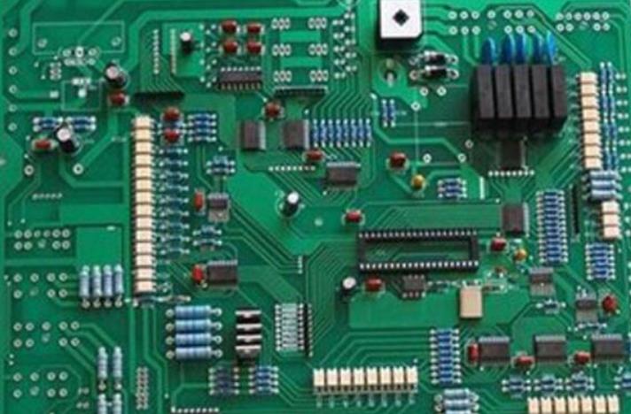
Embedded PCB circuit
With the miniaturization, thin and high-speed electronIC products, the assembly density of PCB components is getting higher and higher, and the transmission rate of electrical signals is getting faster and faster It is difficult to meet the higher and higher assembly requirements only by adding wiring density and multilayer of PCB
Embedded component circuit board can improve packaging reliability and reduce cost
By embedding a large number of embedded passive components in the printed circuit board, the circuit length between components can be shortened, the power characteristics can be improved, the effective packaging area of the printed circuit board can be increased, and a large number of printed circuits can be reduced. Solder points on the surface of the circuit board to improve the reliability of the package and reduce the cost.
Save product space
If these components are embedded in PCB, the space for installing surface mount devices (SMDs) with the same area of PCB will be greatly increased, and the demand for impedance matching of signal transmission characteristics can also be improved. In recent years, PCB of passive components such as embedded resistors and capacitors has been developed rapidly.
Circuit board

Although some technologies are not perfect at present, their advantages are increasingly valued by the electronic manufacturing industry It has become one of the development directions of PCB. It will become more and more mature and widely used
Type assembly pcb of embedded passive components
Embedded passive component PCB can be divided into the following four types according to the type and method of embedded components:
Embedded resistor PCB (embedded resistor PCE), the passive components embedded in PCB are resistors.
Embedded capacitor PCI (embedded capacitor PCI), the passive components embedded in PCB are capacitors.
Embedded Inductive PCB (Embedded Inductive PCB). The passive components embedded in PCB are inductors.
PCB embedded with various passive components is calLED embedded passive PCB (embedded passive PCB).
When two or three resistors, capacitors and inductors are embedded in a PCB, the board can be called a PCB embedded with passive components.
1. Scope of application
Embedded passive component PCB has a wide range of applications. At present, it is mainly used in domestic and foreign computers (such as supercomputers, information processors), PC cards, IC cards and various terminal equipment, communication systems (such as cellular transmission platforms). ATM system, portable communication equipment, etc.), test instruments and test equipment (such as IC scanning cards, interface cards, load plate testers), aerOSPace electronic products (such as space shuttles, electronic equipment on satellites, etc.), consumer electronic equipment (such as potentiometers, heaters), medical electronic equipment (such as scanners, CTs), and military equipment in electronic control systems (such as cruise missiles, radar unmanned reconnaissance aircraft, shields, etc.)
2. Advantages and disadvantages
A large number of passive components that can be embedded are embedded in PCB (including HDI board) to make PCB components more compact and lighter. Embedded passive component PCB has the following advantages:
(1) Increase PCB density
Because discrete (non embedded) passive components not only have a large number of assemblies, but also occupy a large amount of space on the PCB. For example, GSM mobile phones contain more than 500 passive components, accounting for about 50% of the PCB panel assembly area. If 50% of the passive components are embedded in the PCB (or HDI board) for calculation, the size of the PCB board can be reduced by about 25%, thus greatly reducing the number of vias, and the connecting lines will also be reduced and shortened. It can not only increase the flexibility and freedom of PCB design and wiring, but also reduce the amount of wiring and shorten the length of wiring, thus greatly improving the high density of PCB (or HDI board) and shortening the signal transmission path
(2) Improve the reliability of PCB assembly
Inserting the required passive components into PCB can significantly improve the reliability of PCB (or HDUBUM) components. Because through this process method, the number of solder joints (SMTAK PHT) on the PCB surface is greatly reduced, which improves the reliability of the assembly board and greatly reduces the probability of failure caused by solder joints.
In addition, embedded passive components can effectively "protect" to improve reliability. Because these embedded passive components are embedded in PCB as a whole, they are different from discrete (or discrete) passive components with pin welding (or bonding)
The connecting pad on the PCB surface will no longer be corroded by moisture and harmful gases in the air, thus reducing or damaging passive components. This method of embedding passive components can significantly improve the reliability of PCB assembly
(3) Improve the electrical performance of PCB assembly
By embedding passive components in high-density PCBs, the power efficiency of electronic interconnects has been significantly improved. Because it eliminates the connection pads, wires and their leads required for the formation of loops after welding of discrete passive components. Any such circuit will inevitably produce parasitic effects, namely parasitic capacitance and parasitic inductance. With the increase of signal frequency or pulse square wave lead time, this parasitic effect will become more serious. Eliminating such faults will undoubtedly improve the power efficiency of PCB components (greatly reducing signal transmission distortion). At the same time, since the passive components are buried in the printed circuit board, the surrounding environment is closely protected, and their functional values (resistance, capacitance and inductance) will not change due to the dynamic changes of the working environment, making them in a very stable state. This helps to improve the functional stability of passive components and reduce the probability of functional failure of passive components.
(4) Save product manufacturing costs
Using this process method can significantly save product cost or PCB components For example, in the study of the radio frequency circuit (EP-RF) model with embedded passive components, the PCB substrate equivalent to the low profile co fired ceramic substrate (LTCC) (the same passive components are embedded specifically), according to the statistics of the component cost Save 10%, the substrate cost can be saved 30%, and the assembly (consolidating) cost can be saved 40% At the same time, because the assembly process and sintering process of ceramic substrate are difficult to control, and the PCB substrate embedding passive components (EP) can be completed by the traditional PCB manufacturing process, the production efficiency is greatly improved


