SMT inspection, rework and cleaning requirements
<I href="/tw/PCB assembly. html" target="_blank">PCBA inspection and rework
1. Assembly inspection tools:
5 to 10 times magnifier with halo
Printing process standard, eliminating confusion
It may take 10 to 30 times a mICroscope to check difficult parts, such as fine pitch parts and solder paste quality.
For mass production, automated visual inspection, such as 3D laser scanning or X-ray scanning, may be reasonable.
2. Assembly inspection technology:
When checking for residual contaminants or J-wires, you need to tilt the circuit board to check under the components In addition, if rework and repair are carried out at the same time of inspection, a circuit board positioning table may be useful
When in doubt, toothpicks or pointed sticks can be used to verify the solder joints of leaded parts. Use a pick or stick to gently push the upper edge of the wire to check that the connector is connected. This prevents damage to the circuit board and wiring. Unwelded wires or wires with cold joints move when pushed, which requires modification.
Write down or record all defect types using common vocabulary. This information helps identify common defects and trends in order to identify and eliminate their root causes.
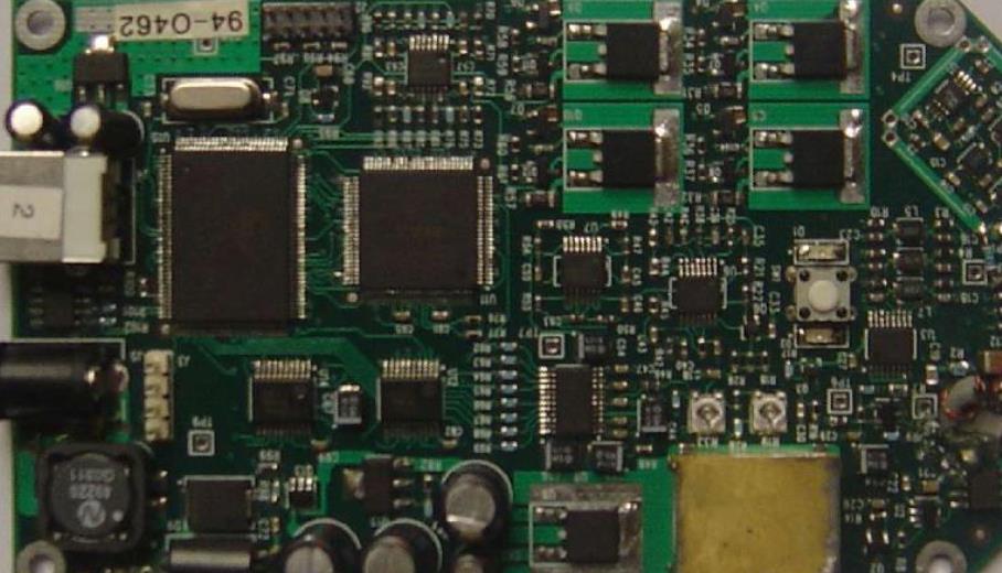
Circuit board

Good solder joints:
Smooth and shiny. There are no voids and pores.
Good solder joint wettability
Concave fillet shape, without excessive solder deposition.
3. Grinding, rework and repair:
Components/circuit boards that do not meet process or performance standards need to be reworked or repaired.
Common rework tools include soldering iron, desoldering station using suction, hot air gun, welding core, etc.
Rework of SO and other high lead packaging requires prior training, and some dummy exercises will help.
Because SMT package leads and terminals are SMAll, compared with through-hole component pads, the thermal requirements are lower. Remove the components only after ensuring that all wires have been desoldered or the solder has returned. If not handLED correctly, the gasket area may be damaged.
Before disassembling the part, gently push the part to check whether the solder is completely melted.
When the connecting solder on each lead or terminal of the component melts, it can be easily removed and replaced with a new one.
Operator training is required because it requires new technologies and tools.
4. Tools required:
Alcohol in dispensing bottle
Cotton swab
"R" and "RMA" fluxes are packed in a small dispensing bottle
Toothpick or pointed stick
Fine tweezers
According to the required core size
Provide thin end temperature control soldering iron and spare parts as required
Unsoldering station in proper position
Manual hot air nozzle and nozzle and hot air rework station
Solder paste and distributor
No. 24 (0.015 – 157;) Flux cored wire
Anti static workstation with wrist strap and proper grounding
SMT Cleaning and Cleaning Option Requirements
1. Cleaning requirements
Printed circuit boards need to be cleaned to remove flux residues and other contaminants left after welding. Cleaning or cleaning the circuit board can prevent potential power failures due to electromigration. Cleaning operations can remove the following contaminants:
i) Ionic contaminant
Ii) Non ionic pollutants
Iii) Particulate pollutants
Water soluble fluxes usually produce ionic (also known as polar) contaminants that need to be cleaned with water. Nonionic (also called non-polar) contaminants produced by rosin flux require non-ionic solvents, such as 3-chloroethane.
2. Cleaning options
Note: Rosin and rosin slightly activated (RMA) flux need not be cleaned. However, for high reliability applications and aesthetic considerations, these boards may need to be cleaned.
As there are corrosive elements in the flux residue, the water-soluble flux needs to be thoroughly cleaned, and water-based cleaning is the ideal choice. Because rosin is insoluble in water, when water-based cleaner is used as rosin flux, an alkaline chEMIcal called saponifier will be added to the water. If ultrasonic vibration is used to assist cleaning, the efficiency of cleaning treatment will be significantly improved. However, ultrasonic vibration is not only limited to the cleaning solution and the surface to be cleaned, but also spreads to the electronIC components that may be damaged. If the bonding line is free and not tightly encapsulated in plastic or any other packaging material, the bonding line in the active component between the chip and the pad may break. High power and high frequency vibrations can also cause external wire breakage. The following parameter sets are generally accepted:
Maximum frequency 40 kHz
Maximum ultrasonic loading time 1 to 5 minutes
Maximum power 10 W/L
The boards are placed on the shelf so that they do not touch each other.
In all cases, the time interval between SMT welding and cleaning should be shortened to the shortest (less than one hour) to obtain a good cleaning effect


