High frequency PCB design and layout considerations
1. What are the skills of high frequency Circuit PCB design?
The design of high frequency circuit board is a complex process, and many factors may directly affect the working effICiency of high frequency circuit. High frequency circuit design and wiring are very important to the whole design. The following ten tips for high frequency circuit PCB design are especially recommended:
One, multilayer PCB wiring
High frequency circuits often have high integration and high wire density. The use of multilayer boards is not only a necessary condition for wiring, but also an effective means to reduce interference. In the PCB layout stage, reasonable selection of PCB size with a certain number of layers can make full use of the middle layer to set the mask, better realize the nearest grounding, effectively reduce the parasitic inductance, and shorten the signal transmission length. All these methods are conducive to the reliability of high-frequency circuits, such as reducing the amplitude of signal cross interference. Some data show that when using the same data, the noise of the four layer board is 2.0 dB lower than that of the double-sided board. However, there is also a problem. The higher the number of PCB half layers, the more complex the manufacturing process, and the higher the organizational cost. This requires us to select a PCB board with an appropriate number of layers when executing PCB layout. Reasonable component layout planning, and use the correct routing rules to complete the design.
Secondly, the SMAller the wire bending between the pins of high-speed electronic equipment, the better
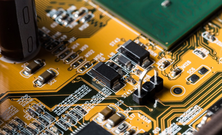
Circuit board

The wiring of high frequency circuits should preferably use full straight lines and need to be rotated. It can be rotated by 45 degree polylines or arcs. This requirement is only used to improve the fixed strength of copper foil in low-frequency circuits, while in high-frequency circuits, it can meet this requirement. One requirement can reduce the external transmission and mutual coupling of high-frequency signals.
3. The shorter the lead between the pins of high-frequency circuit components, the better
The radiation intensity of the signal is proportional to the track length of the signal line. The longer the high-frequency signal wire is, the easier it is to couple with the components close to it. This requires that the signal clock, crystal oscillator, DDR data, LVDS cable, USB cable, HDMI cable and other high-frequency signal cables be as short as possible.
Fourth, the less alternating lead layers between pins of high-frequency circuit components, the better the effect
The so-calLED "less interlaminar alternating of the leads, the better" means that the fewer vias used in the component connection process, the better. From the side, a through-hole can generate 0.5pF distributed capacitance. Reducing the number of through-holes can significantly improve the speed and reduce the possibility of data errors.
2. What PCB layout should be noted between the two
PCB board wiring
The layout of the printed circuit shall be as short as possible, especially in the high-frequency circuit; The bending of the printed wire shall be round, and the right angle or sharp angle will affect the power efficiency and high wire density of the high-frequency circuit; When two panels are connected, the conductors on both sides shall be vertical, inclined or bent to avoid being parallel to each other and reduce parasitic coupling; The use of printed wires as input and output of circuits shall be avoided as far as possible. To avoid reverberation, it is best to add a ground wire between these wires.
Width of printed wire
The width of the conductor shall meet the power efficiency requirements and facilitate production. The minimum value is determined by the current it bears, but the minimum value should not be less than 0.2mm. In high-density and high-precision printed circuits, the wire width and spacing are usually 0.3mm; In case of large current, the temperature rise of conductor width shall also be considered. The single board experiment shows that when the thickness of copper foil is 50mm, the wire width is 1, the current is about 1.5mm, and the current is 2A, the temperature rise is very small. In this case, the conductor with a width of 1~1.5mm can meet the design requirements without causing temperature rise.
The common ground wire of printed wire shall be as thick as possible. If possible, use lines larger than 2 to 3 mm. This is particularly important in circuits with microprocessors. Because when the local line is too thin, the ground potential changes due to the change of current flow, and the level of the microprocessor timing signal is unstable, which will reduce the noise tolerance; For the wiring between IC pins of DIP package, the principle of 10-10 and 12-12 is that when two wires pass between two pins, the diameter of the pad can be set to 50mil, and the line width and line spacing are both 10mil. When only one wire passes between two pins, the diameter of the pad can be set to 64mil, and the line width and line spacing are both 12mil.


