Code for design of LED switching power supply PCB
In any switching power supply design, the physICal design PCB is a link If the design method is improper, this PCB board may EMIt too much electromagnetic interference, causing unstable power operation The following points are analyzed for attention in each step:
1. Design process to establish component parameters from schematic diagram to PCB ->Input principle netlist ->Design parameter setting ->Manual layout ->Manual cabling ->Validate design ->Review ->CAM output
2. The spacing between adjacent conductors in parameter setting must meet the electrical safety requirements. In order to facilitate operation and production, the spacing should be as wide as possible The spacing shall be at least suitable for the voltage When the wiring density is low, the spacing of signal lines can be increased appropriately For signal lines with high level and low level differences, the spacing shall be as short as possible, and new spacing shall be added The distance between the inner hole edge of the pad and the edge of the printed board shall be greater than 1mm to avoid defects of the pad during processing When the wire connected to the pad is relatively thin, the connection between the pad and the wire is designed as a water drop The advantage is that the mat is not easy to peel off, but the wire and mat are not easy to disconnect
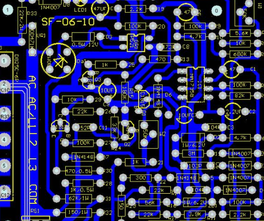
PCB board

3. Practice has proved that even if the circuit schematic diagram is correctly designed and the printed circuit board is improperly designed, the reliability of electronic equipment will be adversely affected For example, if two thin parallel lines of the printed board are close together, the signal waveform will be delayed and reflection noise will be generated at the end of the transmission line The interference caused by power supply and grounding wire will reduce the efficiency of the product Therefore, correct methods should be paid attention to when designing printed circuit boards Each switching power supply has four current loops:
(1) Ac circuit of power switch
(2) Output rectifier AC circuit
(3) Input signal source current loop
(4) Output load current loop The input loop charges the input capacitor through an approximate DC current; SIMilarly, the output filter capacitor is used to store high-frequency energy from the output rectifier and eliminate the DC energy in the output load circuit Therefore, the terminals of input and output filter capacitors are very important The input and output current circuits can only be connected to the power supply from the terminal blocks of the filter capacitor If the connection/output circuit between inputs and the power switch/rectifier circuit cannot be directly connected to the terminal of the capacitor, AC energy will pass through the input or output filter capacitor and radiate to the environment The AC circuit of the power switch and rectifier contains high amplitude trapezoidal current, high order harmonIC components, and the frequency is much higher than the fundamental frequency of the switch The peak amplitude can reach 5 times of continuous input/output DC current The transition time is usually about 50ns For double circuits vulnerable to electromagnetic interference, the power supply in other printed circuits must be laid in front of these AC circuits. Each circuit has three main components of filter capacitors, power switches or rectifiers, inductors or transformers, which should be placed adjacent to each other. Adjust the current path between component positions to make it as short as possible The design process is as follows:
Design the input current source Loop and input Filter Design the output load loop and output filter According to the functional units of the circuit, the layout of all the components of the circuit should comply with the following principles:
(1) First consider the size of the PCB When the size of a PCB board is too large, the print line length, impedance and noise resistance will increase, and the cost will increase; The heat dissipation is too SMAll, and adjacent lines are vulnerable to interference The circuit board is rectangular with a length ratio of 3:2 or 4:3. The distance between the components at the edge of the circuit board and the edge of the circuit board is generally not less than 2mm
(2) place the device to consider the future welding
(3) To the components of each functional circuit as the center The components shall be evenly, neatly and compactly arranged on the PCB board to minimize and shorten the wires and connections between components. The decoupling capacitor shall be as close to the VCC of the device as possible
(4) For circuits working at high frequencies, the distribution parameters between components should be considered In general circuits, components shall be arranged in parallel as far as possible With this kind of pipe, it is not only beautiful, but also easy to install, weld and mass produce
(5) Arrange the position of each functional circuit unit according to the circuit process
(6) The first principle of layout is to ensure the distribution rate of wiring
(7) reduce the loop area as far as possible to suppress the radiation interference of switching power supply.
4. The wiring switch power supply contains high-frequency signals, and the PCB can act as an antenna The length and width of the printed circuit will affect its impedance and inductance, thus affecting the frequency response Even printed lines that pass through dc signals can be coupled to rf signals from adjacent printed lines and cause circuit problems (or even re-radiate interference signals). This means that all components connected to the printed circuit and other power lines must be closely placed together The length of a printed circuit is proportional to its inductance and impedance, and the width is inversely proportional to its inductance and impedance The length reflects the wavelength of the print line response The longer the length, the lower the frequency of the printing line, which can send and receive electromagnetic waves, and it can radiate more RF energy According to the current of the printed circuit board, increase the width of the power line as much as possible to reduce the circuit resistance At the same time, turn on the power cord, and the ground wire and current are in the same direction, which helps to enhance the anti noise ability Grounding is the bottom branch of the four current loops of switching power supply. It plays a very important role as the common reference point of the circuit, which is an important method to control interference Therefore, carefully consider the grounding cable in the layout Mixing ground cables may cause power supply instability The following points should be paid attention to in the design of ground cables:
4.1. Normally, the single point grounding is correctly selected. The common side of the filter capacitor should couple another grounding to the contact with large current. The grounding should be close to the circuit, and the corresponding circuit filter capacitor can also be placed on the leveling ground. The main consideration is that the current part is grounded, and the circuit is changing. The reason for introducing interference is that the actual impedance of the circuit will cause the ground potential of each part of the circuit to change In this switching power supply, its inductance has less influence between wiring and components, while the grounding circuit has greater influence on the formation of circulating current interference. In addition, single point grounding is used, The power switch current loop (in the ground of several devices are connected to the ground on his feet), the grounding of the output rectifier current loop of several devices also receives the corresponding filter capacitor grounding. With this kind of pipeline, the power supply works stably and is not easy to self excite. It is impossible to do this at all. In fact, two diodes or a small resistance in total can be connected to a more concentrated copper foil
4.2. If the grounding wire is very thin, the grounding wire should be thickened as much as possible. The grounding potential changes with the current, the timing signal level of electronic equipment is unstable, and the anti noise efficiency is poor. In summary, ensure that each high current grounding terminal uses short and wide printed wire as much as possible, and try to expand the power supply range, the width of the grounding wire, and the width of the grounding wire than the power line. Their relationship is: ground wire> The power cord & gt; Signal lines, if possible, the width of ground wire should be greater than 3mm. Large area copper layer can also be used for grounding, and printed boards are not used for grounding The following principles should also be followed:
(1) Wiring direction: from the welding surface, the Layout of components should be consistent with the schematic diagram as much as possible, and the wiring direction should be consistent with the wiring direction of the circuit diagram, because in the production process, it is usually necessary to detect various parameters of the welding surface, so it is easy to do in the production inspection, debugging and maintenance (note: Refers to meet the circuit performance and machine installation and panel layout requirements under the premise.
(2) When designing the wiring diagram, the line should turn as little as possible, the line width on the printed arc should not be changed, and the wire corner should be greater than 90 degrees, so as to make the lines concise and clear
(3) The printed circuit is not allowed to have cross circuit That is, a wire, a capacitor, and a transistor at the bottom of the gap are introduced from other resistors to "drill" through them, or they may "wind" through the intersection of a wire. Under special circumstances, how complex the circuit is. In order to simplify the design, wire bridging is also allowed to solve the cross circuit problem Because a single panel is used, the in-line components are located on the upper surface and the surface mounting devices are located on the lower surface. In the layout process, the tandem components can overlap the surface mount devices, but the use of pads should be avoided
4.3. Low voltage DC-DC input and output switching power supply returns the voltage echo to the main transformer. The circuits on both sides should have a common reference. Therefore, after laying copper wires on both sides of the grounding wire, they are also connected to form a common point
5. Check whether the wiring design is completed, carefully check whether the wiring design of the designer meets the requirements, and also confirm whether the rules meet the requirements of the PCB production process. For general wire to wire inspection, the distance between lines and component pads, lines and communication holes, component pads and communication holes, through holes and through holes is reasonable, and whether they meet the Production requirements Whether the width of power line and ground wire is appropriate, and whether there is PCB board with widened ground wire Note: Some errors can be ignored. For example, some contours of some connectors are placed outside the board frame; In addition, it must be re coppered every time the wiring and holes are modified
he above is the explanation given by the editor of pcb circuit board company.
If you want to know more about PCBA, you can go to our company's home page to learn about it.
In addition, our company also sells various circuit boards,
High Frequency Circuit Board and SMT chip are waiting for your presence again.


