design of High Speed PCB Based on CADence
1. The introduction
The responding high-speed printed circuit board is used more and more widely, and the design is more and more complex With the increase of communICation demand, the speed of signal transmission and processing is faster and faster High speed circuit has two meanings: first, the frequency is very high It is generally believed that the frequency of digital circuit reaches or exceeds 45MHz to 50MHz, and the circuit working at this frequency accounts for one third of the whole system, so it is calLED high-speed loop In addition, considering the rise and fall time of the signal, when the rise time of the signal is less than 6 times of the signal transmission delay, the signal is considered as a high-speed signal, which is independent of the specific frequency of the signal
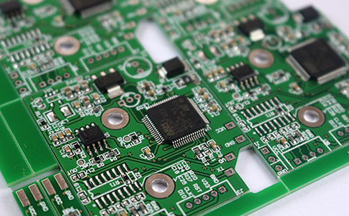
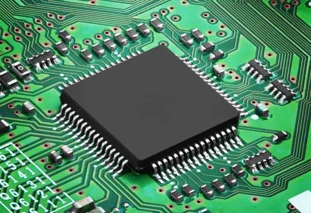
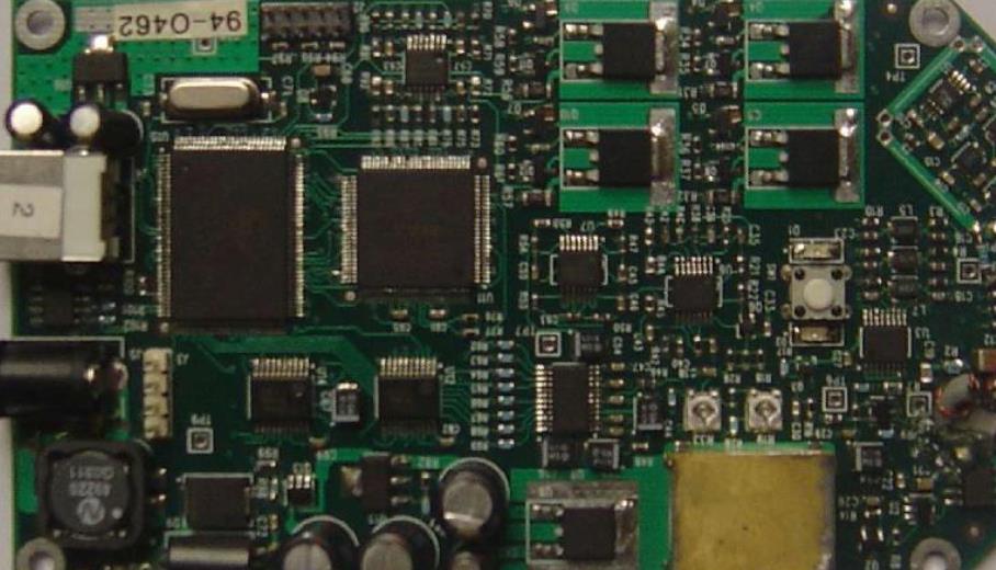
PCB board

2. Basic content High speed PCB design
High speed circuit design in the modern circuit design of the promotion is more and more large. It is increasingly difficult to design. Its solution requires not only high-speed equipment, but also the wisdom and meticulous work of designers. We must carefully study and analyze specific situations to solve the existing high-speed circuit problems Generally speaking, the design mainly includes three aspects: signal integrity design, electromagnetic compatibility design, and power integrity design
2.1 Signal is in the tegrity design
Signal integrity refers to the quality of the signal on the signal line. A signal with good signal integrity means that it has the necessary voltage level to achieve when needed The poor signal integrity is not caused by any one factor, but many factors are comprehensively considered in the design at the board level Especially in high-speed circuits, the switching speed of chips used is too fast, the layout of terminal components is unreasonable, and the interconnection of circuits is unreasonable, which will lead to signal integrity problems It mainly includes crosstalk, reflection, overshoot and drop, oscillation, signal delay, etc
2.1.1 Crosstalk (crosstalk)
Crosstalk is the unnecessary coupling between two adjacent signal lines. Mutual inductance and tolerance between signal lines will cause noise on the line Therefore, it is divided into inductive crosstalk and capacitive crosstalk, which generate coupling current and coupling voltage respectively When the edge rate of signal is lower than 1ns, crosstalk shall be considered If an AC signal current passes through the signal line, it will generate an alternating magnetic field, and the adjacent signal lines in the magnetic field will sense the signal voltage General parameters PCB board layer, distance between signal lines, power characteristics of driver and receiver, and connecting pipes of signal lines all have certain influence on crosstalk In Cadence signal analogy tool, six coupled signal lines can be analogized SIMultaneously after crosstalk The scanning parameters that can be set are: dielectric constant PCB, dielectric thickness, thickness of immersed copper, length and width of signal line, and signal line spacing In analogy, it is necessary to specify the damaged signal line, that is, investigate the interference of another signal line to this line, and set the excitation to a constant high or constant low. In this way, the sum of the induced voltages of other signal lines to this signal line can be measured to make the spacing and parallel length meet the requirements
2.1.2 Reflex (reflection)
Reflection is the echo of a signal along a transmission line. As we know, when light passes through a discontinuous medium, part of its energy is reflected back At this point, not all signal power is transmitted to the load, but some is reflected back In a high-Speed PCB, the conductor must be equivalent to the transmission line According to the transmission line theory, if the power supply and load have the same impedance, reflection will not occur The impedance miSMAtch between the two will cause reflection, and the load will reflect part of the voltage back to the power supply The reflected voltage may be positive or negative, depending on the relationship between load impedance and source impedance If the reflected signal is strong and superimposed on the original signal, it may change the logic state, resulting in receiving data errors If the clock signal may cause the clock edge to be monotonous, then trigger the wrong trigger General wiring geometry, wire termination errors, transmission through connectors, and discontinuities in the power plane all cause this reflection In addition, there are usually multiple receiver outputs. Then, the reflection generated by different cabling strategies has different effects on each receiver. In this regard, cabling strategies can not be ignored
2.1.3 Overshoot and undershoot
Overshoot is a signal jump caused by too fast circuit switching and the reflected above, that is, the signal peak exceeds the peak or valley value of the set voltage The downdraft is the next trough or crest Overrush will lead to protection diode operation, premature failure and serious equipment damage Excessive downlink will cause false clock or data errors, which can be reduced or eliminated by adding appropriate endpoints
2.1.4 Oscillations and Pawnchess
The phenomenon of oscillation is the repeated occurrence of overshoot and downshot. The signal oscillation and surrounding oscillation are caused by the impedance mismatch between the receiving end and the transmission line, while the source end is caused by the excessive inductance and capacitance on the line, usually near the threshold value of the logic level. Crossing the threshold value of the logic level for many times will lead to logic dysfunction Oscillation and circumferential oscillation are caused by reflection and other factors. By properly terminating or changing PCB parameters, oscillation can be reduced, but not completely eliminated In Cadence's signal simulation software, the above signal integrity problems are measured in reflection parameters In the IBIS model, we only need to set different transmission line impedance parameters for the driver device and the receiving repository, and we can use the simulation tool to directly calculate the signal waveform and corresponding data, so that we can find the matching transmission line impedance value, opposition, and signal transmission rate, the width of the corresponding signal line in each layer can be obtained according to the corresponding transmission line impedance value and signal transmission rate (the order and parameters of lamination need to be set in advance). There are many ways to choose resistance matching, including source end to end and parallel end to end, etc In terms of wiring strategy, different pipes can also be selected: chrysanthemum, artiste, custom. Each method has its advantages and disadvantages. Specific choices are determined according to different circuit simulation results
2.1.5 Signal Delay
The circuit can only receive data in accordance with the specified time sequence. Too long signal delay may lead to confusion of timing and functions. In low-speed systems, there will be no problem, but the signal edge rate and clock frequency increase, and the transmission time and synchronization time between devices will be shortened Overload of the drive and long wiring will cause delay All gate delays must be met in an increasingly short time budget, including set times, hold times, line delays and deflections Because the equivalent capacitance and inductance on the transmission line will delay the digital switching of the signal and couple with the oscillating winding caused by reflection, the data signal cannot meet the time required for the receiving equipment to receive correctly, resulting in receiving errors In Cadence signal simulation software, signal delay is also measured in reflection sub parameters, settlement test, Switchdelay and Propdelay The first two parameters are related to the test load in IBIS model base These two parameters can be determined manually by the driver and the user of the receiver equipment They can be compared with the analogue settling delay and switching delay If the switch delay value obtained in the slow mode is less than the calculated value, and the switch delay value obtained in the fast mode is greater than the calculated value, then we can get the delay range between the two devices that we really need During the placement of specific equipment, if the equipment is not in the proper position, the part of the corresponding delay table will display red. After the correct position adjustment, it will turn blue, indicating that the delay between equipment has met the specified delay range
2.2 Design for Electro Magnetic Compatibility
Electromagnetic compatibility includes excessive electromagnetic radiation and sensitivity to electromagnetic radiation There are two kinds of electromagnetic interference: conducted interference and radiated interference Conducted interference refers to the signal transmitted from one power grid to another through the conductive medium in the form of current In PCB board, mainly including grounding noise and power noise Radiated interference means that signals radiate out in the form of electromagnetic waves and affect another power grid In the design, high-speed PCB boards and systems, high-frequency signal lines, chip pins, connectors, etc. may become radiation interference sources with antenna characteristics According to the importance of EMC design, it can be divided into four levels: equipment level and PCB level design, grounding system design, mask system design and filter design Among them, the first two are very important. The level design of equipment and PCB mainly includes the selection of active components, circuit board stacking, layout and wiring The design of grounding system mainly includes grounding pipe, grounding impedance control, grounding loop and shielding layer grounding In Cadence simulation tool, the analog parameters of electromagnetic interference can be in X, Y, Z direction of distance, frequency range, design margin, compliance with standards, etc This kind of comparison belongs to the latter analogy, which mainly checks whether the design requirements are met. Therefore, in the preliminary work, we also need to design according to the electromagnetic interference theory. The common practice is to control the electromagnetic interference design rules applied to each link of the design, so as to realize the rule driving and control of each link
2.3 Power integrity design
In high-speed circuit, power and ground integrity is also a very important factor, because power integrity and signal integrity are closely related In most cases, the main cause of signal distortion is the power supply system For example, excessive ground bounce noise, inappropriate design of decoupling capacitor, poor division of multiple power sources or grounding layers, unreasonable design of layers, and uneven current distribution will bring power supply integrity problems, leading to signal distortion and affecting signal integrity The main idea to solve this problem is to determine the distribution system, divide the large size circuit board into several small size circuit boards, determine the decoupling capacitance according to the ground bounce noise, and consider the PCB board as a whole When there is a large current flowing through the circuit, if a large number of chip outputs are turned on at the same time, there will be a large transient current in the chip from the flat panel power supply. The chip packaging and the resistance and inductance of the power plane will cause power noise, which will not produce voltage fluctuations and changes in the actual ground plane, and the noise will affect other parts of the action In the design, reducing the load capacitance, adding load resistance, and reducing the grounding inductance and the number of switches can reduce the grounding elasticity Due to the division of the ground plane, for example, the stratum is divided into digital ground, analog ground, mask ground, etc, When the digital signal reaches the analog ground area, it will generate ground plane return noise At the same time, depending on the selected equipment, the power supply layer can be divided into several different voltage layers. In addition, special attention should be paid to ground bite and return noise The selection of distribution system and decoupling capacitor is very important in power integrity design Generally, keep the impact between the power supply system (power supply and ground plane) as low as possible We can determine the desired target impedance by specifying the voltage and current variation range, and then adjust the relevant factors in the circuit to make the impedance of all parts of the power supply system consistent with the target impedance For decoupling capacitors, it is necessary to consider the parasitic parameters of capacitors, calculate the number of decoupling capacitors, the capacitance of each capacitor and the specific location, and try not to exceed one capacitor and not less than one capacitor In Cadence simulation tool, ground bounce is called simultaneous switching noise In the analogy, the capacitance and resistance between the parasitic inductance, power supply and parasitic inductance are considered, and the results are more consistent with the actual situation In addition, according to the circuit type and operating frequency used by the system, after setting the required parameters, the appropriate capacitance size and placement position can be calculated, and a low impedance grounding circuit can be designed to solve the PCB board problem


