
Crosstalk measurement method for PCB quality verifICation
With the continuous improvement of the running speed of digital systems in the field of communications, video, network and computer technologies require more and more pcb product quality printed circuit boards in such systems In the face of increasing signal frequency and shortening pulse rise time, the design of early PCB board could not guarantee the system performance and working requirements In the current PCB design, we need to use the transmission line theory to analogy PCB board and its components (edge connector, microstrip line, and component sockets) Only by fully understanding the form, the mechanism and consequences of crosstalk on PCBs, and using corresponding technologies to suppress it, can we help us improve the reliability of systems including PCBs This paper focuses on PCB design, but I believe the content discussed in this paper will also be useful in other applications, such as cable and connector characteristics PCB designers are concerned about crosstalk because it can cause performance problems, such as new noise levels, unwanted SPIkes, data edge jitters, and unexpected signal reflections Which problems will affect the PCB design depends on many factors, such as the characteristics of the logic circuit used on the circuit board, the design of the circuit board, the mode of crossover (reverse or forward), as well as interference lines and interference lines Terminals on both sides of the conductor The information provided below can help readers improve their understanding and research of crosstalk, thus reducing the impact of crosstalk on the design
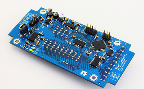
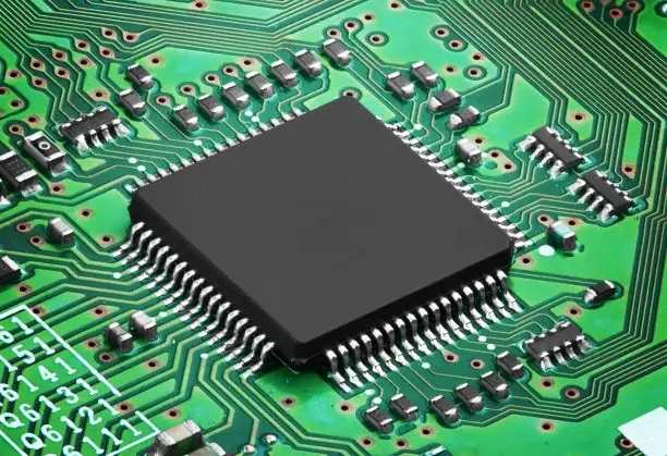
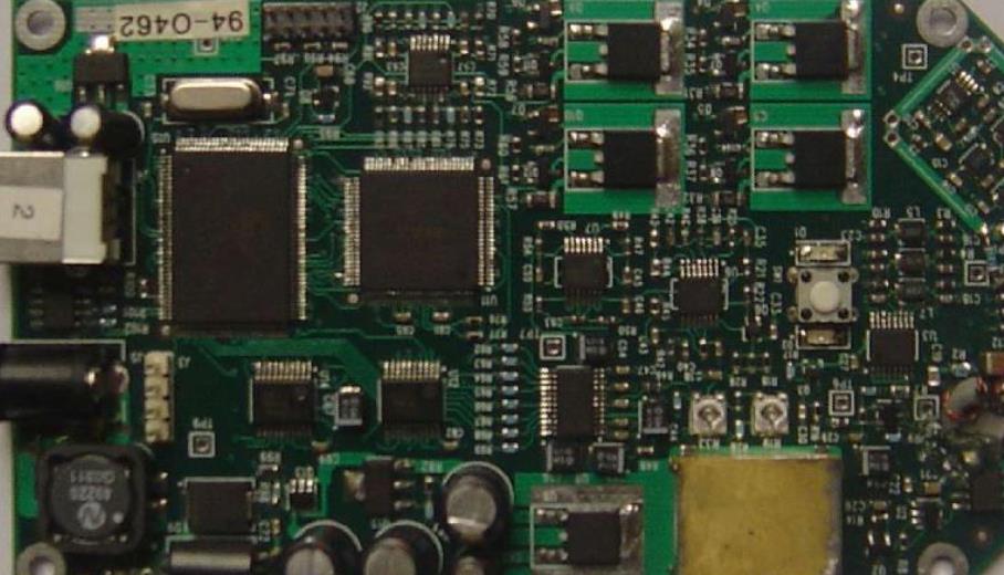
PCB board
Methods of studying crosstalk
In order to minimize crosstalk in PCB design, we must find a balance between capacitive reactance and inductive reactance, and strive to reach the rated impedance value, because PCB requires that the transmission line impedance be well controlLED After the circuit board design is completed, the components, connectors, and terminals on the circuit board determine the impact of the crosstalk type on the circuit efficiency Using time-domain measurement, by calculating the corner frequency and understanding the PCB crosstalk (Crosstalk on PCB board) model, it can help designers set the limits of crosstalk analysis
Time Domain Measurement Methods
To measure and analyze crosstalk, frequency domain technology can be used to observe the relationship between the harmonIC components of the clock in the spectrum and the EMI values at these harmonic frequencies However, the time domain measurement of digital signal edges (the time it takes to rise from 10% to 90% of the signal level) is also a means of measuring and analyzing crosstalk Therefore, the signal speed (ie, rise time) defined by the signal edges can also help restore the mechanism of crossover The rise time can be directly used to calculate the corner frequency This paper describes and uses rise time measurement method to measure crosstalk
Knee frequency
To ensure reliable operation of a digital system, designers must study and verify the circuit design efficiency lower than corner frequency The frequency domain analysis of digital signals shows that signals above knee frequency will attenuate, which will not have a substantial impact on crosstalk, while signals below knee frequency contain enough energy to affect circuit operation The knee joint frequency is calculated by the following formula: fknit=0.5/rise time
PCB crosstalk model
The models presented in this section provide a platform for the study of different forms of crosstalk and illustrate how the mutual impedance between two microstrip lines can cause crosstalk on a PCB. The mutual impedance is evenly distributed along the two traces Crosstalk occurs when the digital gate hits a rising edge to the crosstalk line and propagates along the trace:
1) Both the mutual capacitance Cm and the mutual inductance Lm will couple or "crosstalk" a voltage to the adjacent disturbed line.
2) The crosstalk voltage appears on the disturbed line in the form of a narrow pulse whose width is equal to the rise time of the pulse on the disturbing line.
3) On the distorted line, the crosstalk pulse is divided into two and starts to spread in two opposite directions The crosstalk is divided into two parts: forward crosstalk propagating in the direction of the original interference pulse and reverse crosstalk propagating in the direction opposite to the signal source
Types of Crosstalk and Coupling Mechanisms
Based on the model discussed earlier, the following describes the coupling mechanism of crosstalk, as well as two types of crosstalk, forward and backward, and discusses
Interference mechanism caused by mutual capacitance in the circuit:
When the pulse on the disturbing line reaches the capacitor, the narrow pulse will be coupled to the disturbed line through the capacitor The amplitude of the coupling pulse is determined by the mutual capacitance Then, the coupling pulse is divided into two parts and starts to propagate along the disturbed line in two opposite directions
Inductive or Transformer Coupling Mechanisms
Mutual inductance in a circuit can cause disturbances such that a pulse propagating on the disturbance wire will charge the next location where the current spike is present. This current spike generates a magnetic field and then a current spike on the disturbed wire The transformer produces two voltage spikes of opposite polarity on the disturbed line: the negative spike propagates forward and the positive spike propagates backward
reverse crosstalk
The capacitively and inductively coupled crosstalk voltages caused by the above model have an additive effect at the crosstalk location of the disturbed wire. The resulting reverse crosstalk has the following characteristics: reverse crosstalk is the sum of two pulses with the same polarity Since the crosstalk position propagates along the edge of the interference pulse, the reverse interference is displayed as low level. The width of the wide pulse signal at the source end of the interfered line corresponds to the length of the track The reflected crosstalk amplitude is independent of the rise time of the interference line pulse, but depends on the mutual impedance value
forward crosstalk
To reiterate, the crosstalk voltage of capacitive coupling and inductive coupling is accumulated at the crosstalk position of the disturbed line Forward crosstalk includes the following characteristics: Forward crosstalk is the sum of two reverse polarity pulses Because the two poles are opposite, the result depends on the relative value of capacitance and inductance The forward crosstalk appears at the end of the disturbed line in the form of a narrow spike, and its width is equal to the rise time of the attack pulse The forward crosstalk depends on the rise time of the interference pulse The faster the rising speed, the higher the amplitude and the narrower the width The forward crosstalk amplitude also depends on the pair length: because the crosstalk position propagates along the edge of the intrusion pulse, the forward crosstalk pulse on the disturbed wire will gain more energy
Instruments and Setup
To effectively measure crosstalk in the laboratory, a broadband oscilloscope with a measurement bandwidth of 20 GHz shall be used. The circuit under test shall be driven by a high-quality pulse generator whose output pulse rise time is equal to the rise time of the oscilloscope At the same time, high-quality cables, termination resistors and adapters are used to connect the PCBs under test The TDR step voltage generator can generate a narrow pulse of 250mv with a rise time of 17ps and an output source impedance of 50 ohms The tester only needs to connect the PCB to be tested
Forward Crosstalk Measurement
If only measuring forward crosstalk, terminate all traces to eliminate reflection The forward crosstalk shall be measured at the end of the well terminated disturbed line The instrument setting is shown in Figure 6
The effect of circuit design on crossover
Although crosstalk can be reduced and its effects observed or eliminated through careful PCB design Therefore, proper line end load should also be used when designing circuits, because line end load will affect the magnitude of crosstalk and the degree of crosstalk attenuation over time How does the line end load at the end of the trace and at the logic gate output attenuate crosstalk and reduce its cause


