Influence of PCB layout inductance on converter effICiency
As the computer industry moves towards providing up to 200A DC-DC converters at 1V, PCB layout technology needs to meet the requirements of this challenging emerging converter Comparing the effects of various wiring defects, we focus on the effects of parasitic inductance in the circuit, especially those related to the source, drain, switch MOSFET and gate We built a PCB to test the DC-DC converter receiving 12V DC and converting it to 1. 3V and up to 20A output The inductance of each MOSFET electrode can be changed individually or SIMultaneously at any time by using the chip board for assembly We choose to use the inductance value as the percentage of the total inductance of the professionally designed 2-inch circuit board, rather than the actual value, because the wiring personnel only know the length of a specific track, not necessarily know its inductance value
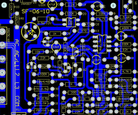
PCB board

Test Design
We use the converter efficiency to measure the effectiveness of these parasitic inductors. This is because efficiency is the standard to measure the efficiency of DC-DC converter. The test is divided into the following parts: adjust the proportional coefficient of each inductance value of MOSFET drain, source and gate, and observe the impact on the synchronous rectifier by measuring the conversion efficiency. Through the combination of any of the above two, understand the relationship between them. The inductance of the inductance test board is 43nH, which is usually set as 0%, 25%, 50% and 100%. In our experiment, the parasitic resistance on the inductance test board has little effect and can be ignored. Since the harmful effects of parasitic inductance depend on the frequency, we conducted experiments at three preset switching frequencies: 300kHz, 600kHz and 1MHz. This shows us how important the design of switching from normal switching frequency to higher frequency will be in the future. As we all know, in the power circuit, the length of all traces must be kept short to avoid voltage and current ringing, reduce the overall electromagnetic interference of the circuit board, and avoid negative effects on "more stable" components in the circuit (especially analog control circuits and related components). In addition, reference data show that the source inductor controlling MOSFET has a nonlinear effect on the increase of source current drop time, resulting in higher power consumption and lower conversion efficiency. In addition to the above phenomena, the source inductance may also cause ringing at the switch node.
Test circuit and circuit board
The circuit used is a synchronous rectifier topology operating in an open loop. This is to eliminate any influence that the control loop may have on the circuit efficiency, and enable us to focus on power conversion efficiency, especially MOSFET efficiency. We know that high inductance conditions can cause serious ringing, especially at switch nodes. Select a gate driver IC that can withstand such ringing without adverse effects. This Four layer circuit board uses two ounces of copper data, and the internal two layers are the grounding and power layers. All rules for good wiring shall be followed when wiring.
Influence of grid inductance
At the switching frequency of 300 kHz, the grid inductance has little effect on the efficiency. At 600kHz switching frequency, the influence of grid inductance is more obvious, and the efficiency changes 1.2% at 20A. At 1MHz, the efficiency degradation almost disappears. We have not investigated this reason, and we can guess that the probability of resonance factor offsetting its loss is 50%. The resonant phenomenon of MOSFET gate drive should be further studied. We observe that the gate inductance has little effect on the efficiency of controlling and synchronizing MOSFETs.
Influence of source inductance
The source inductance has a more significant effect on the efficiency. In some cases, we have to stop the test before reaching the current because the temperature of the MOSFET is higher than 130 ℃. Figure 5 shows the results of the control MOSFET study. A careful examination of these results shows that the DC-DC converter cannot operate at full 20A at a frequency of 300kHz and 100% inductance because the MOSFET temperature exceeds 130 ° C. It can also be found at 50% inductance, 600kHz and 1MHz. It is observed that the efficiency degradation caused by the source inductance is more serious than that without the source inductance. When the inductance is 50% and the current is 15A, the efficiency will be reduced by 7% even at the switching frequency of 300 kHz. When the inductance is 100%, the efficiency decreases to 11%. At the switching frequency of 600kHz and 1MHz, compared with the situation without source inductor, this effect is more obvious and the efficiency degradation is more serious. Obviously, even the low source inductance will reduce the efficiency, especially when the switching frequency is 600 kHz.
Influence of leakage inductance
Leakage inductance may cause severe ringing, which may be sufficient to cause MOSFET breakdown under extreme conditions (Figure 3). This will also have a negative impact on efficiency. Efficiency is a function of load current and leakage inductance at different frequencies. In addition, the following results can be observed: when the current is 15A, 300kHz and 50% inductance, we must stop the test because the temperature of MOSFET exceeds 130 。 At the same frequency, 100% inductance, we can not get any readings, because the ring is too serious. At 300kHz and 12A, the efficiency of 50% leakage inductance is 7% lower than that of 0%. Due to the high temperature of MOSFET, the test cannot be conducted above 15A. At 600kHz and 12.5A, the leakage inductance efficiency of 50% is 8.5% lower than that of 0%. Because the MOSFET temperature is too high, it cannot be tested above 12.5A. At 1MHz, due to the high temperature of MOSFET, the test cannot be conducted above 5A.
Influence of gate source inductance
A larger source inductance will significantly reduce efficiency. The basic relationship between efficiency and grid inductance has been proved. When combined with a SMAller source inductor, the overall situation becomes very clear - a larger grid inductor necessarily results in a larger power loss. The interpretation of this result needs further study. We can now explain that within the reasonable inductance value range of the circuit board, the leakage inductance and source inductance must be reduced to ensure high converter efficiency. The analogy results are as follows: the gate and source inductors resonate with the gate source capacitor of MOSFETs. When HS-FET turns off the grid source, the capacitor discharges through these inductive paths. After the MOSFET is turned off, the inductance will force the grid current to continue to flow and reverse charge the grid source capacitor. This charge will be discharged again in the same tube and reverse the gate source voltage of HS-FET. Depending on the inclination, HS-FET can be turned on again in the event of a large short circuit. This effect becomes serious at such a high grid inductance. In some cases, the second short-circuit effect can even be seen. As a part of the resonant circuit, the source inductor can also act as a second kind of pipe. When a short-circuit current occurs, the source inductance limits the di/dt (rate of change of current over time) of the short-circuit current, thereby limiting the loss. The source inductance also causes negative feedback to the grid source voltage and limits short circuits. These effects occur especially in areas with high parasitic gate inductances. In order to improve efficiency, this effect should be avoided by design, that is, the grid inductance must be carefully designed to minimize it.
Influence of source HS source LS inductance
We study the effect of the position of the parasitic source inductor on the efficiency. In the same number of parasitic source inductance circuits, the control FET has a greater impact on its efficiency than the synchronous FET. The reason for this phenomenon is that the slow switching control of FET will cause additional switching loss, because the VDS of the control FET is higher than the VDS of the synchronous FET during the conversion (the forward voltage drop of the synchronous FET is very small). In addition, the response of parasitic inductance to the gate drain voltage of FET has a significant effect on the leakage current of the entire HS-FET. In contrast, the parasitic source inductance has only a partial effect on the leakage current of LS-FET, because it can be bypassed by the body diode of synchronous FET.
Effects of Parallel MOSFETs
When MOSFETs are connected in parallel, it is unlikely that each individual MOSFET ring will have the same parasitic in many cases We study the effect of additional inductance in MOSFET drain ring on efficiency We prove the adverse effect of parasitic inductance on switching mosfet efficiency in DC-DC converter through experiments The conclusions are as follows: The inductance in the source circuit has a serious impact, followed by the similar inductance in the drain circuit On our test board, we did not find any serious influence related to the inductance of the grid circuit The reduction of efficiency is closely related to the switching frequency of the converter The reduction of efficiency is closely related to the load current In the case of parasitic inductance in the source and drain circuits, the greater the load current, the greater the efficiency decline In today's DC-DC converter applications, special care must be taken when routing power system PCBs, especially switching MOSFETs One of the advantages of using multilayer plates is to reduce parasitic resistance and inductance by injecting as much current as possible into each layer This reduces resistance losses and losses caused by parasitic inductance When designing high frequency DC-DC converter, there are many parasitic inductance problems in source and drain circuits The first is packaging inductance. It is feasible to switch MOSFETs using the recently introduced low inductance packaging The second item is the parasitic inductance PCB of the motor. Multilayer PCB must be used to reduce the trace inductance This allows designers to use fewer capacitors to achieve faster dynamic response and successful high-frequency design The design cannot avoid the parasitic induction moving into the synchronous FET circuit, because the inductance in the synchronous FET circuit has less influence on the overall efficiency than the inductance in the control FET circuit Note: Under low duty cycle, parasitic resistance in SFET circuit can significantly reduce efficiency Complex trade offs need to be made in the design (trace width, copper thickness, effective loop range, offset, etc.) Avoid parallel MOSFET The way to replace MOSFETs in parallel is to add additional phases or use better MOSFETs If parallel connection cannot be avoided, for parallel MOSFETs, power symmetry must be guaranteed in the design to obtain the same current distribution and the same switching time PCB


