5G era
5G commercial set off a wave of replacement
5G mobile network will surpass the current mobile network in many aspects, mainly including speed, delay, bandwidth and energy consumption. The speed of 5G mobile network will reach 10 gigabits per second, 100 times the current maximum speed; The delay can refer to the time required to wait until receiving the response from the other party. In the current 4G network, the delay is between several milliseconds and one hundred milliseconds, and the delay in the 5G network will be reduced to one millisecond.
However, to enjoy the convenience of 5G communication, you need a terminal that supports it. At present, 100% of the mobile phones in the hands of ordinary users in China do not support it. The arrival of the 5G era will certainly set off a new round of machine replacement boom. As the basis of the electronic industry, PCB industry will also welcome new development opportunities.
PCB laser MARKing tracing
The arrival of the 5G era also puts forward higher requirements for the R&D, production and management capabilities of PCB enterprises. Enterprises must provide more cost-effective products to the market at a faster speed, and improving the traceability efficiency of product management has become a key link.
A complete data traceability system needs to be established for a product from warehousing, production, testing and ex warehouse to achieve internal product quality control. In order to achieve product traceability, the product must be identified with words or bar codes to give the product a unique "ID card".

Traceability identification processing on PCB mainly includes screen printing and laser marking. Silk printing is easy to fall off, easy to remove, rough marks, environmental pollution and other problems. In addition, portable electronic products are increasingly developing towards miniaturization, high integration and portability, and the bonding pads and spacing are becoming SMAller and smaller, making it more difficult to print alignment.
Laser marking, with its accuracy and flexibility, can overcome the technical defects of traditional processing methods such as easy falling off and low processing accuracy, and will play a pivotal role in PCB industry.
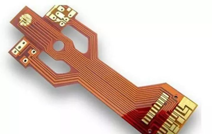
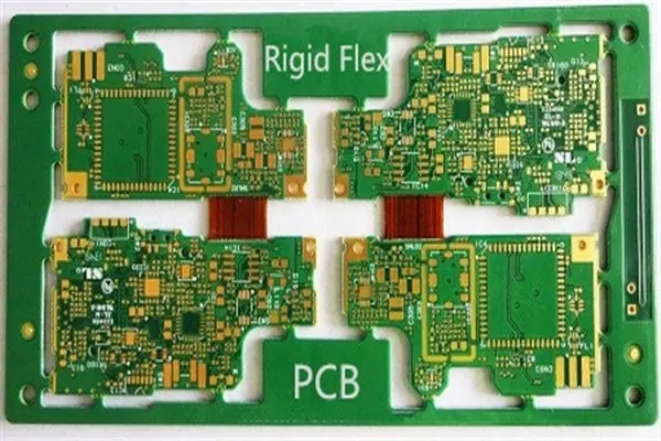
In the electronic industry, Flexible circuit board can be said to be the blood transfusion pipeline of electronic products. In particular, under the trend of electronic equipment being thin and light, miniaturized, wearable and foldable, flexible circuit boards have the advantages of high wiring density, thin and light, bendable, and three-dimensional assembly. They are moderately high in line with the market development trend, and the demand is growing.
The traditional processing methods of FPC include die, V-CUT, milling cutter, stamping, etc., but this is a mechanical contact plate splitting process, which has stress, is prone to produce burrs, dust, and is not accurate enough, so it is gradually replaced by the laser cutting process.
As a non-contact processing tool, laser can be used in a very small focus (100~500 μ m) High intensity light energy (650mW/mm2) is applied on the surface. Such high energy can be used for laser cutting, drilling, marking, welding, scribing and other processing of materials.
Advantages of laser cutting flexible circuit board
● As the line density and pitch of FPC products continue to increase, and the FPC graphic contour is becoming more and more complex, this makes it more and more difficult to make FPC molds. The laser cutting flexible circuit board adopts the numerical control processing form, which does not require mold processing, and saves the mold opening cost;
● Due to the lack of machining itself, the machining accuracy is restricted. The laser cutting flexible circuit board uses high-performance ultraviolet laser light source, with good beam quality and better cutting effect;
● As the traditional processing technology is a contact machining method, it will inevitably produce processing stress on FPC, which may cause physical damage. Laser cutting flexible circuit board is non-contact processing, effectively avoiding damage and deformation of processing materials.
It is predicted that 5G will bring an economic output of 100 billion dollars to PCB industry, and the application of laser technology in PCB industry will also help it seize the opportunity and usher in a new stage of development.


